Semiconductor device and forming method thereof

一种半导体、器件的技术,应用在半导体器件及其形成领域,能够解决电学性能差等问题,达到提高性能、保护能力强、避免漏电的效果

Active Publication Date: 2018-09-25
SEMICON MFG INT (SHANGHAI) CORP +1
View PDF4 Cites 6 Cited by
  • Summary
  • Abstract
  • Description
  • Claims
  • Application Information

AI Technical Summary

Problems solved by technology

[0004] However, the electrical performance of existing semiconductor devices is poor

Method used


Image

  • Semiconductor device and forming method thereof
  • Semiconductor device and forming method thereof
  • Semiconductor device and forming method thereof

Examples


Embodiment Construction

[0031] As mentioned in the background, the electrical performance of semiconductor devices formed in the prior art is relatively poor.

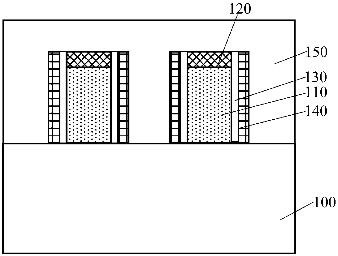
[0032] Figure 1 to Figure 2 It is a structural schematic diagram of the formation process of a semiconductor device.

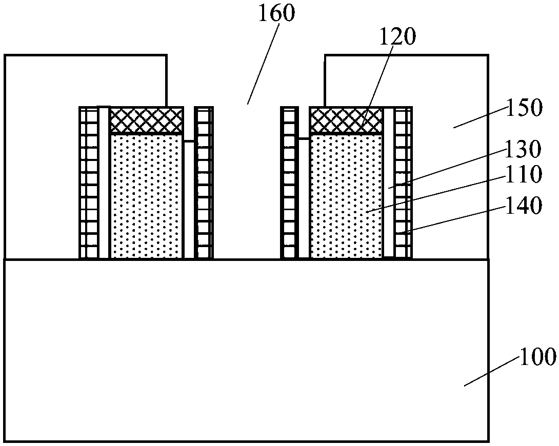
[0033] refer to figure 1 , providing a substrate 100, the substrate 100 has a gate structure 110 and a protective layer 120 on the top surface of the gate structure 110; a first sidewall is formed on the sidewall of the gate structure 110 and the sidewall of the protective layer 120 130; form a second sidewall 140 on the sidewall of the first sidewall 130; form an interlayer dielectric layer 150 on the substrate 100, and the interlayer dielectric layer 150 covers the protective layer 120 and the first sidewall 130 and the second side wall 140 .

[0034] The material of the first sidewall 130 is silicon oxide, and the material of the second sidewall 140 is silicon nitride. Therefore, the electrical isolation performance o...


PUM


Abstract

Disclosed are a semiconductor device and a forming method thereof. The method includes the following steps: providing a substrate, wherein the substrate is provided with gate structures and first protective layers located on the top surfaces of the gate structures; forming initial side walls on the sidewalls of the gate structures and the sidewalls of the first protective layers; forming first side walls on the sidewalls of the initial side walls, wherein the material of the first side walls is different from that of the initial side walls; removing part of the initial side walls after the first side walls are formed so as to form second side walls on the initial side walls, and forming grooves between the first side walls and the first protective layers, wherein the second side walls arelocated at the bottoms of the grooves and the top surfaces of the second side walls are higher than or flush with that of the gate structures; and forming second protective layers in the grooves, wherein the material of the second protective layers is the same as that of the first side walls. The method can improve the electrical properties of semiconductor devices.

Description

technical field [0001] The invention relates to the field of semiconductor manufacturing, in particular to a semiconductor device and a forming method thereof. Background technique [0002] In a semiconductor device, such as a flash memory, there is a gate structure for controlling the channel current, and source and drain doped regions on both sides of the gate structure, and the source and drain doped regions are used to pass through the conductive plug and the The electrical connection of the interconnect layer in the back-end process. Before forming the conductive plug, it is usually necessary to form an interlayer dielectric layer covering the gate structure and the source-drain doped region, and then form a contact hole in the interlayer dielectric layer, and the contact hole is used to accommodate the conductive plug . [0003] As the size between adjacent gate structures is continuously reduced, the size of the contact hole between the gate structures is continuous...

Claims


Application Information

Patent Timeline
Patent Type & Authority Applications(China)
IPC IPC(8): H01L29/423H01L29/40H01L21/28H01L21/331
CPCH01L21/28008H01L29/401H01L29/42364H01L29/6656H01L29/42324H01L21/76897H01L29/40114H01L29/6653H01L21/31111H01L21/31116H01L21/31144H01L21/76802H01L29/0649H01L29/7881H01L29/66825H01L21/02164H01L21/0217H01L29/4916
Inventor 郑二虎邹陆军
Owner SEMICON MFG INT (SHANGHAI) CORP
Why Eureka
Try Eureka