
Base silicon wafer used for preparing cut silicon wafers and preparation method and purpose

A silicon wafer and basic technology, applied in the field of solar cell preparation, can solve problems such as cell fragmentation, and achieve the effects of reducing attenuation, reducing the generation of fine cracks, and prolonging service life

Inactive Publication Date: 2018-09-28
CSI CELLS CO LTD +1
View PDF7 Cites 8 Cited by
  • Summary
  • Abstract
  • Description
  • Claims
  • Application Information

AI Technical Summary

Problems solved by technology

During the slicing process, tiny cracks may occur on the silicon wafer, and these small cracks may extend along the natural cleavage direction of the monocrystalline silicon during the scribing and subsequent processes, eventually causing the cell to break
[0003] This field needs to develop a kind of technical solution that can solve the technical problem of micro-cracks in the slicing process, or produce cell fragmentation

Method used


Image

  • Base silicon wafer used for preparing cut silicon wafers and preparation method and purpose
  • Base silicon wafer used for preparing cut silicon wafers and preparation method and purpose
  • Base silicon wafer used for preparing cut silicon wafers and preparation method and purpose

Examples


Embodiment 1

[0038] A cutting silicon wafer, prepared by the following method:

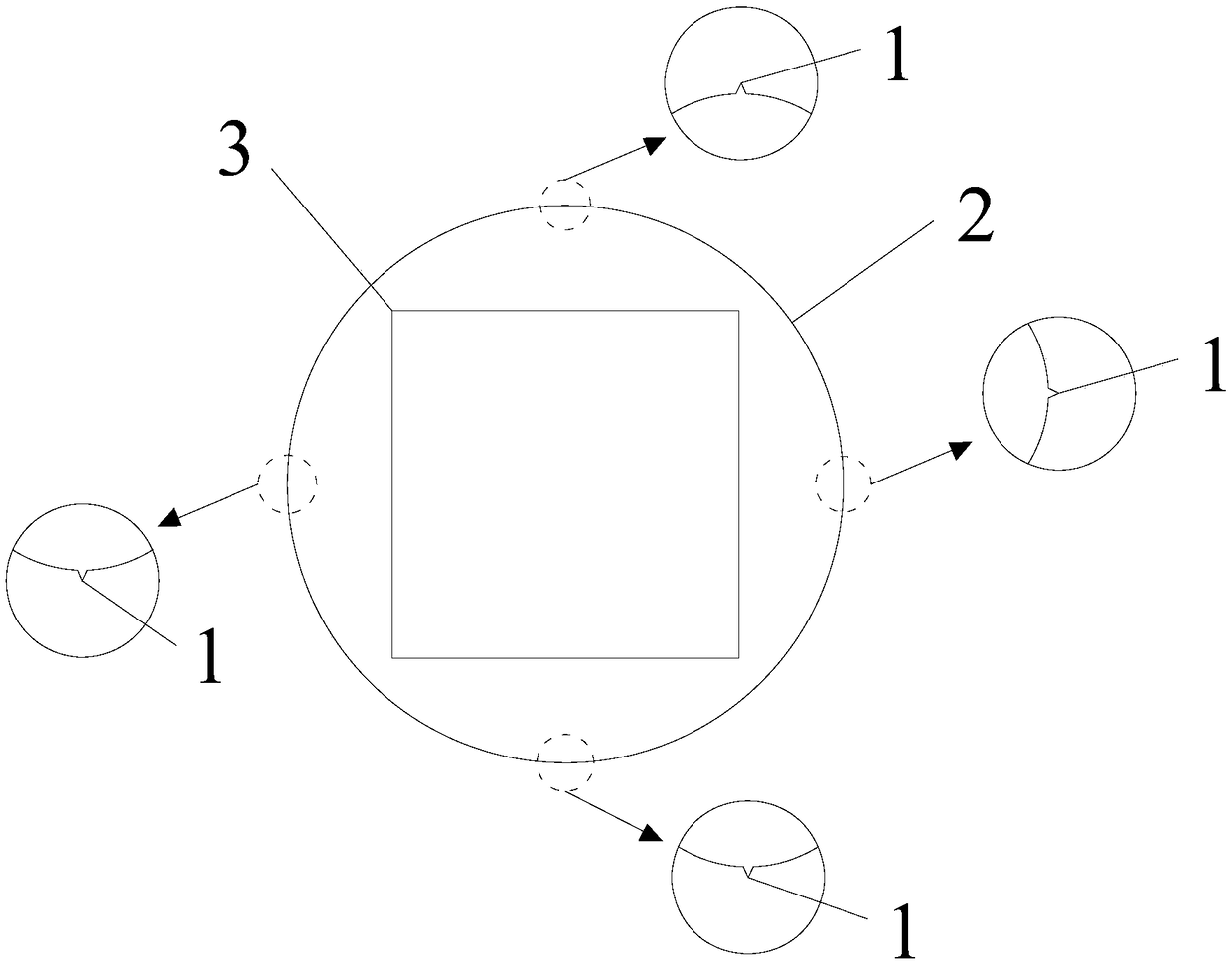
[0039] (1) Take a 0.5m long single crystal silicon rod with a diameter of 220mm and cut it into a silicon square rod with an end face side length of 156mm. The end face of the silicon square rod is parallel to the end face of the single crystal silicon rod. The extension line connecting the midpoint of the side length of the end face of the square rod and the center of the end face of the silicon square rod passes through the point on the cross section of the single crystal silicon rod through the corrugated line;

[0040] (2) According to the predetermined silicon wafer thickness of 180 μm, the silicon square rod is cut to obtain the basic silicon wafer; the surface of the basic silicon wafer is parallel to the end surface of the silicon square rod;

[0041] (3) The basic silicon wafer of step (2) is cut into 2 pieces in a direction parallel to the length of either side, and a total of 20,000 cut silicon wafers are ...

Embodiment 2

[0043] A cutting silicon wafer, prepared by the following method:

[0044] (1) Take a 0.3m long single crystal silicon rod with a diameter of 225mm and cut it into a silicon square rod with an end face side length of 156mm. The end face of the silicon square rod is parallel to the end face of the single crystal silicon rod. The extension line connecting the midpoint of the side length of the end face of the square rod and the center of the end face of the silicon square rod passes through the point on the cross section of the single crystal silicon rod through the corrugated line;

[0045] (2) According to a predetermined silicon wafer thickness of 120 μm, the silicon square rod is cut to obtain a basic silicon wafer; the surface of the basic silicon wafer is parallel to the end surface of the silicon square rod;

[0046] (3) Cut the basic silicon wafer of step (2) into 4 pieces in a direction parallel to the length of any side, and cut a total of 40,000 cut silicon wafers, which hav...

Embodiment 3

[0049] A cutting silicon wafer, prepared by the following method:

[0050] (1) Take a 0.6m long single crystal silicon rod with a diameter of 220mm and cut it into a silicon square rod with an end face side length of 156mm. The end face of the silicon square rod is parallel to the end face of the single crystal silicon rod. The extension line connecting the midpoint of the side length of the end face of the square rod and the center of the end face of the silicon square rod passes through the point on the cross section of the single crystal silicon rod through the corrugated line;

[0051] (2) According to the predetermined silicon wafer thickness of 220 μm, the silicon square rod is cut to obtain the basic silicon wafer; the surface of the basic silicon wafer is parallel to the end surface of the silicon square rod;

[0052] (3) Cut the basic silicon wafer of step (2) into 2 pieces in a direction parallel to the length of any side, and cut a total of 20,000 pieces of cut silicon waf...


PUM

PropertyMeasurementUnit
thicknessaaaaaaaaaa
thicknessaaaaaaaaaa

Abstract

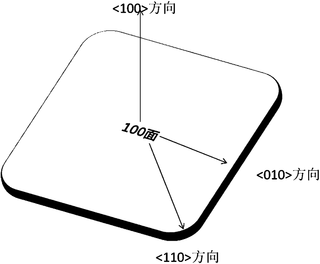
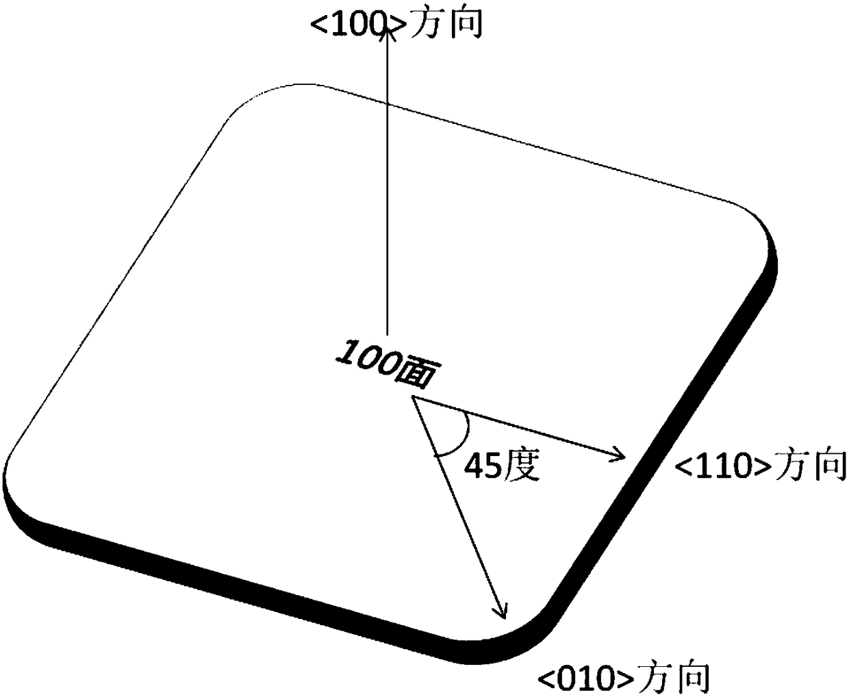
The invention relates to a base silicon wafer used for preparing cut silicon wafers. The surface of the base silicon wafer is in the shape of a square or a square provided with chamfers. The projection of the natural cracking direction of the base silicon wafer on the surface of the base silicon wafer is parallel to a pair of opposite sides of the base silicon wafer. The base silicon wafer is a monocrystalline silicon wafer. According to the base silicon wafer used for preparing the cut silicon wafers, the projection (110) of the natural cracking direction of the base silicon wafer on the surface of the base silicon wafer is parallel to the pair of opposite sides of the base silicon wafer, when the base silicon wafer is used for preparing the cut silicon wafers, the crack direction is in the direction parallel to the sides of the base silicon wafer, the wafer breaking rate can be decreased, and the wafer cutting direction is unchanged; and occurring of fine cracks of cutting positionsis reduced, attenuation of an assembly can be effectively reduced, and the service life of the assembly is prolonged.

Description

Technical field [0001] The invention belongs to the field of solar cell preparation, and in particular relates to a basic silicon wafer for preparing cutting silicon wafers, and a preparation method and application. Background technique [0002] In order to increase the module power of solar cells, slicing technology is introduced at the module end, that is, the cells are divided into two or more parts, and then solder ribbons are used in series and parallel. Slicing the battery can reduce the current of the component, thereby reducing the loss of series resistance. Slicing is usually performed by heating and scribing the surface of the cell with the high energy of a laser, and then mechanically breaking the silicon wafer into two along the scribing direction. During the slicing process, the silicon wafer may have tiny cracks, and these small cracks may extend along the natural cleavage direction of the monocrystalline silicon during the dicing and subsequent processes, and even...

Claims


Application Information

Patent Timeline
Patent Type & Authority Applications(China)
IPC IPC(8): B28D5/00H01L31/18C30B29/06
CPCB28D5/00C30B29/06H01L31/18Y02P70/50
Inventor 刘运宇蒋方丹王栩生邢国强
Owner CSI CELLS CO LTD
Learn More