Anti-radiation MOSFET structure having P-type island buffer layer structure

A buffer layer, anti-radiation technology, applied in the direction of electrical components, circuits, semiconductor devices, etc., can solve the problem of too much higher, increase the on-resistance of power MOSFET, etc.

Active Publication Date: 2018-09-28
BEIJING UNIV OF TECH
View PDF3 Cites 1 Cited by
  • Summary
  • Abstract
  • Description
  • Claims
  • Application Information

AI Technical Summary

Problems solved by technology

In order to ensure good results, the concentration of the buffer layer should not be much higher than the concentration of the withstand voltage layer, and at the same time, the concentration of the buffer layer must ensure a certain thickness, which will undoubtedly increase the on-resistance of the power MOSFET

Method used


Image

  • Anti-radiation MOSFET structure having P-type island buffer layer structure
  • Anti-radiation MOSFET structure having P-type island buffer layer structure

Examples


Embodiment 1

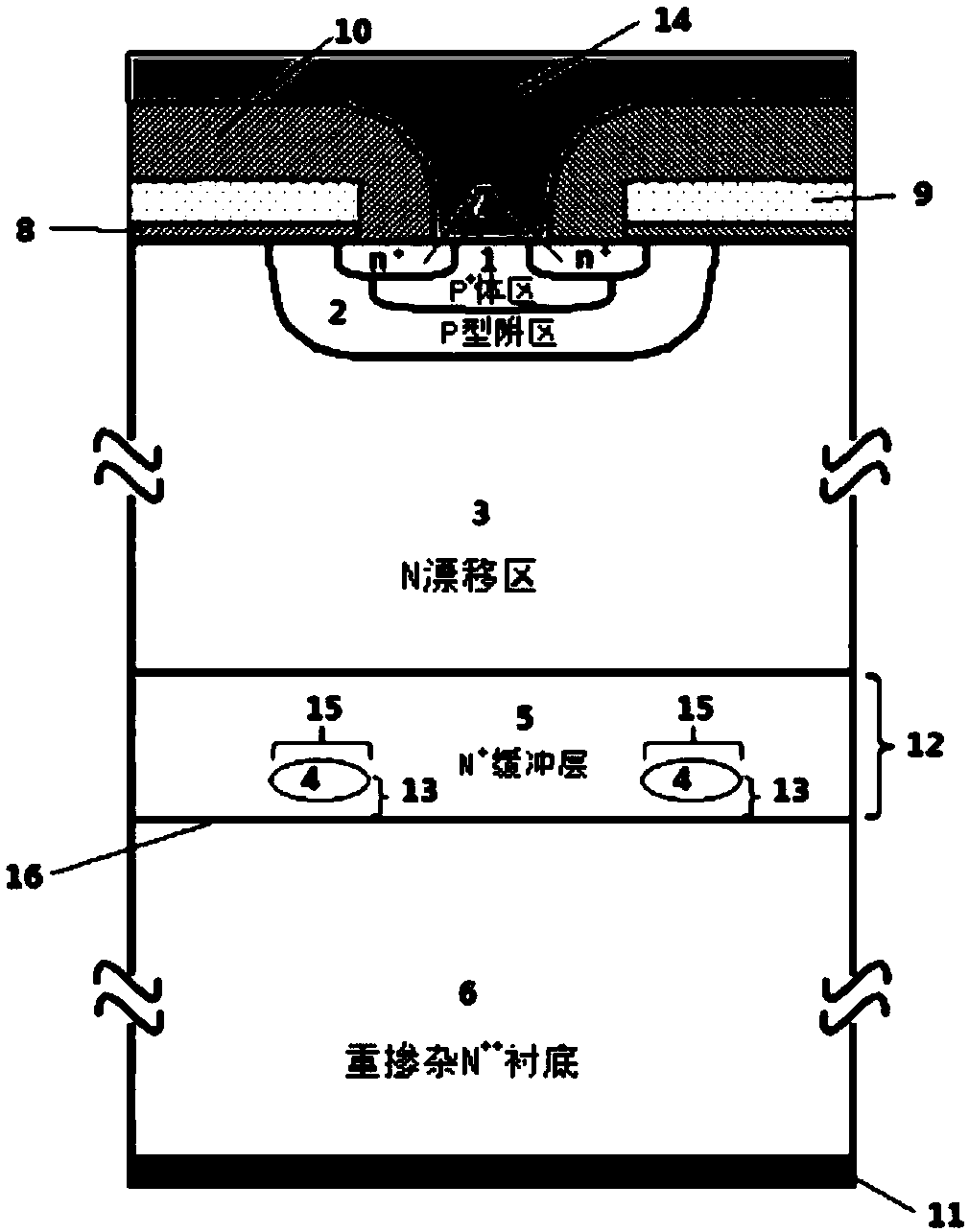
[0013] This embodiment is a planar gate MOSFET with a P-type island buffer layer structure. figure 1 . In its structure, except for the P-type island buffer layer that embodies the characteristics of the present invention, the others are the same as the common planar gate MOSFET structure: N ++ The substrate (6) has a thickness of 100 microns and is doped with arsenic at a concentration of 2×10 19 cm -3 ; The thickness of buffer layer (5) is 15 microns, doping concentration 5 * 10 16 cm -3 ; The thickness of the drift region (3) is 15 microns, and the doping concentration is 1×10 15 cm -3 ; P-type well region (2) is generated by diffusion, with a junction depth of 2.5 microns; P + Body region(1) junction depth 1.2 µm, N + The junction depth of the source region (7) is 0.5 micron; the channel length determined by the diffusion difference between the well region and the source region is about 1.8 micron. The repetition period of the cells on the silicon wafer is 12 micro...

Embodiment 2

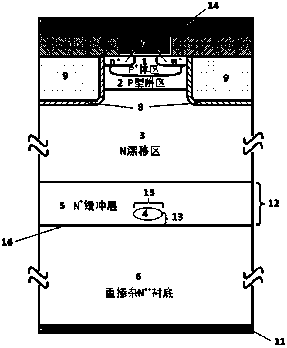
[0015] This embodiment is a trench gate MOSFET with a P-type island buffer layer structure. The cell structure is square. For the cross-sectional structure of the device, refer to the attached figure 2 . In its structure, except for the P-type island buffer layer that embodies the characteristics of the present invention, the others are the same as the common planar gate MOSFET structure: N ++ The substrate (6) has a thickness of 100 microns and is doped with arsenic at a concentration of 2×10 19 cm -3 ; The thickness of buffer layer (5) is 15 microns, doping concentration 5 * 10 16 cm -3 ; The thickness of the drift region (3) is 15 microns, and the doping concentration is 1×10 15 cm -3 ; P-type well region (2) is generated by diffusion, with a junction depth of 2.5 microns; P + Body region(1) junction depth 1.2 µm, N + The junction depth of the source region 7 is 0.5 microns; the channel length determined by the diffusion difference between the well region and the so...


PUM


Abstract

The invention discloses an anti-radiation MOSFET (Metal-Oxide-Semiconductor Field Effect Transistor) structure having a P-type island buffer layer structure. The anti-radiation MOSFET structure is characterized in that: a buffer layer with a P-type island structure is added between a substrate and a drift region of a conventional power MOSFET structure; the concentration of the buffer layer is between a doping concentration of the drift region and a doping concentration of the substrate, the concentrate and the size of the P-type island are controlled strictly, so that an unipolar mode is ensured when a device is in a conducting state; at the same time, when the device is in a blocking state, the P-type island can adjust an electric field adjacent to a buffer layer-substrate high-low junction, so as to improve a feedback effect induced by a parasitic BJT (Bipolar Junction Transistor) when the device is subjected to single particle radiation, thereby raising an SEB (Single Event Burnout) threshold. The invention provides a novel structure capable of improving an anti-SEB capacity for a spacial power MOSFET.

Description

technical field [0001] The invention belongs to power semiconductor switching devices, specifically a radiation-resistant MOSFET structure based on silicon materials with a P-type island buffer layer structure, which has a certain anti-burning ability when irradiated by high-energy charged particles, and is suitable for use with single-particle radiation. According to the space work environment. Background technique [0002] As an important switching device in power electronics technology, metal oxide semiconductor field effect transistor (MOSFET) is widely used in various power electronic equipment to perform power conversion and processing such as rectification, inverter, boost, step-down, and frequency conversion. At the same time, relying on the excellent performance of the device and relatively mature technical advantages, the power MOSFET is also considered to be one of the most satisfactory devices in the field of space electronic system applications, and is widely us...

Claims


Application Information

Patent Timeline
Patent Type & Authority Applications(China)
IPC IPC(8): H01L29/06H01L29/78
CPCH01L29/0684H01L29/7827
Inventor 胡冬青唐伯晗贾云鹏吴郁张靖维
Owner BEIJING UNIV OF TECH
Why Eureka
Try Eureka