Heavily doped semiconductor-based broadband terahertz absorber

An absorber and terahertz technology, which is applied in the field of broadband terahertz absorbers, can solve problems such as the inability to achieve ultra-broadband absorbing effects, and achieve the effect of easy integration and simple graphics

Inactive Publication Date: 2018-10-16
HARBIN UNIV OF SCI & TECH
View PDF3 Cites 15 Cited by
  • Summary
  • Abstract
  • Description
  • Claims
  • Application Information

AI Technical Summary

Problems solved by technology

[0003] With the development of modern information warfare, the research of terahertz absorber has attracted more and more attention. Terahertz absorber refers to a device that can absorb most of the energy of the incident terahertz band electromagnetic wave and convert the energy into Other forms of energy can achieve a class of special materials with almost no reflection. In 2014, W Withayachumnankul...

Method used


Image

  • Heavily doped semiconductor-based broadband terahertz absorber
  • Heavily doped semiconductor-based broadband terahertz absorber
  • Heavily doped semiconductor-based broadband terahertz absorber

Examples


Embodiment Construction

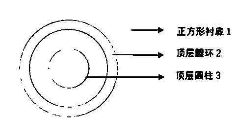
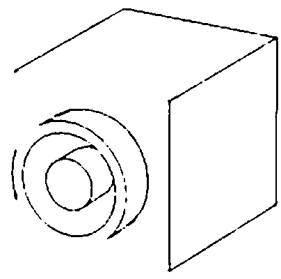
[0021] refer to figure 1 , figure 2 It can be seen that the present invention is based on highly doped P-type silicon to form a structure with a period of 200 μm, wherein the cube 1 is the substrate, and a layer of circular ring 2 and cylinder 3 with the same doping concentration of 50 μm in thickness is superimposed on it. Concentration of 6.8´10 17 cm -3 , and then according to the theoretical calculation method of the Drude model, the carrier mobility is calculated to be 200cm 2 / (VS), the conductivity is about 0.055Ω·cm, the outer radius of the ring is 75μm, the inner radius is 60μm, and the radius of the cylinder is 35μm. It can be seen from the figure that the top layer of highly doped silicon structure is similar to a plasma The resonator supports the surface plasmon mode; when the terahertz beam is vertically incident on the structure, it can excite the surface plasmon polaritons (SPPs) of the structure and generate localized surface plasmon resonance, which enha...


PUM

PropertyMeasurementUnit
Doping concentrationaaaaaaaaaa
Thicknessaaaaaaaaaa

Abstract

The invention discloses a heavily doped semiconductor-based broadband terahertz absorber, which is formed by a two-layer structure, wherein a top layer is formed by a circular ring and a cylinder; a substrate is a cube; used materials for the broadband terahertz absorber all are highly doped semiconductors of the same doping concentration; and a plasma material is formed through heavy doping on aterahertz band on the basis of a silicon material, thereby achieving the characteristic that electromagnetic waves entering the surface of the structure are almost completely absorbed. The heavily doped semiconductor-based broadband terahertz absorber has the characteristics of being simple in structure, free of multiple layers of materials for stacking, convenient to process, insensitive in polarization, high in absorption efficiency, relatively wide in absorption band and wide-angle in absorption, and can basically meet the application requirements for the terahertz absorption aspect.

Description

technical field [0001] The invention belongs to a broadband terahertz absorber based on highly doped semiconductors, and belongs to the application field of highly doped semiconductors in the terahertz band. Background technique [0002] Terahertz waves are between microwave and infrared light in the electromagnetic spectrum, and the wavelength is usually 30 μm ~ 3mm. Terahertz waves include electromagnetic waves with frequencies between 0.1 and 10 THz. Terahertz radiation has long been considered safer radiation, especially compared to X-rays. It can penetrate many commonly used dielectric materials such as paper, leather, plastic, wood, etc., and because of its relatively low photon energy, it will not cause obvious damage to organisms, so terahertz waves are widely used in semiconductors; Medical science; national defense security and information technology and other fields. However, in some fields, it is still necessary to avoid the influence of terahertz radiation, so...

Claims


Application Information

Patent Timeline
IPC IPC(8): H01Q17/00G02B5/00
CPCG02B5/003H01Q17/008
Inventor 朱冬颖王玥崔子健
Owner HARBIN UNIV OF SCI & TECH
Why Eureka
Try Eureka