Solar cell and manufacturing process thereof

A solar cell and manufacturing process technology, applied in the field of solar cells, can solve problems affecting the improvement of photoelectric conversion efficiency, etc., and achieve the effect of high photoelectric conversion efficiency

Active Publication Date: 2018-10-19
ZHANGJIAGANG GCL INTEGRATION TECH CO LTD +1
View PDF5 Cites 2 Cited by
  • Summary
  • Abstract
  • Description
  • Claims
  • Application Information

AI Technical Summary

Problems solved by technology

But no matter how good the passivation is, the existence of recombination centers is inev...

Method used


Image

  • Solar cell and manufacturing process thereof

Examples


Embodiment 1

[0043] Prepare a solar cell with a double-sided symmetrical emitter junction structure:

[0044] (1) Alkali texturing of silicon wafers: cleaning of N-type monocrystalline silicon wafers to remove the damaged layer on the surface of the silicon wafers, followed by alkali texturing, the lye used is according to KOH: additive: H2O=8:1.5 : The KOH solution prepared in the ratio of 160, the concentration of the KOH solution is 5%, the temperature is 80° C., and a pyramid structure suede is formed on both sides of the silicon wafer;

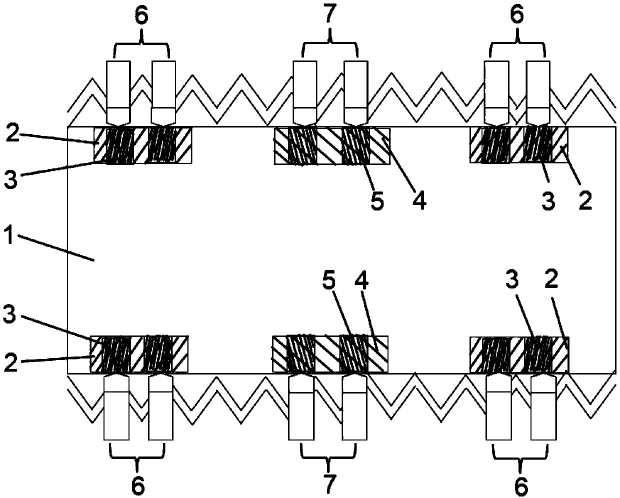
[0045] (2) Form symmetrical p+ regions on both sides of the battery: First, use boron tribromide as the boron source in the boron diffusion furnace to perform single-sided boron diffusion. Wax to prepare mask, and then pass through HF / HNO in single-side etching equipment 3 The solution etches away the boron in the area not covered by the mask, thereby forming a p+ region in the covered area. The p+ region is located on the left and right sides of bot...


PUM

PropertyMeasurementUnit
Square resistanceaaaaaaaaaa

Abstract

The invention relates to a solar cell and a manufacturing process thereof. A silicon wafer of the solar cell is an N-type single crystal silicon wafer or a P-type single crystal silicon wafer, a silicon wafer surface has a pyramid structure suede, and front and back surfaces of the silicon wafer have electrodes and emitter junctions; the emitter junctions are formed by p+ regions and n+ regions onthe silicon wafer surface. At the same time, the invention also discloses a manufacturing process of the solar cell. According to the above solar cell, since both the front and back surfaces have PNjunctions, the generated photogenerated carriers are quickly collected under the action of a built-in electric field, and do not need to pass through the entire silicon wafer substrate, which can effectively improve photoelectric conversion efficiency and avoid the thermal decay phenomenon of P-type single polycrystalline PERC batteries and Al-BSF batteries. Moreover, due to the characteristics ofthe double-sided emission junctions, in the actual power generation process, there will be two peak outputs in one day, the power generation amount is high, and the power generation cost is significantly reduced.

Description

technical field [0001] The invention relates to the technical field of solar cells, in particular to a solar cell with double-sided emitter junctions and a manufacturing process thereof. Background technique [0002] As a new energy source, solar energy has the advantages of being inexhaustible, clean and environmentally friendly compared with traditional fossil fuels. Solar power generation devices, also known as solar cells or photovoltaic cells, can directly convert solar energy into electrical energy. The principle of power generation is based on the photovoltaic effect of semiconductor PN junctions. When light reaches the surface of the cell, it is absorbed to generate electron-hole pairs. That is, the photogenerated carriers, under the action of the built-in electric field, the photogenerated carriers must pass through the entire silicon wafer substrate to be collected. During this crossing process, photogenerated carriers will inevitably be captured by recombination ...

Claims


Application Information

Patent Timeline
IPC IPC(8): H01L31/0236H01L31/0352H01L31/068H01L31/18
CPCH01L31/02363H01L31/03529H01L31/0684H01L31/1804Y02E10/547Y02P70/50
Inventor 崔艳峰袁声召张淳
Owner ZHANGJIAGANG GCL INTEGRATION TECH CO LTD
Why Eureka
Try Eureka