A Method for Preparing Perovskite Thin Films Based on Anti-Solvent Dynamic Spin Coating

A perovskite and anti-solvent technology, applied in semiconductor/solid-state device manufacturing, semiconductor devices, electrical components, etc., can solve the problems of fine grains of perovskite thin films, and achieve the effect of flat and dense surface and reduced loss.

Active Publication Date: 2020-05-12
UNIV OF ELECTRONICS SCI & TECH OF CHINA
View PDF3 Cites 0 Cited by
  • Summary
  • Abstract
  • Description
  • Claims
  • Application Information

AI Technical Summary

Problems solved by technology

This method can effectively control the crystallization process of perovskite so that the perovskite film layer has good compatibility with the mesoporous substrate, but the prepared perovskite film has fine grains.

Method used


Image

  • A Method for Preparing Perovskite Thin Films Based on Anti-Solvent Dynamic Spin Coating
  • A Method for Preparing Perovskite Thin Films Based on Anti-Solvent Dynamic Spin Coating
  • A Method for Preparing Perovskite Thin Films Based on Anti-Solvent Dynamic Spin Coating

Examples


Embodiment 1

[0034] A method for preparing a perovskite film based on anti-solvent dynamic spin coating, specifically comprising the following steps:

[0035] Step 1. Clean the substrate:

[0036] 1.1 will bring TiO 2 The FTO conductive glass of the electron transport layer was ultrasonically cleaned in acetone, alcohol, and water for 20 minutes respectively, and dried in a vacuum drying oven;

[0037] 1.2 For the treated TiO in the previous step 2 The FTO conductive glass of the electron transport layer is subjected to 20min UV-ozone treatment to increase the hydrophilicity of the substrate;

[0038] Step 2, take lead iodide as solute, DMF as solvent, stir 12h, prepare the lead iodide solution that mass concentration is 0.416g / mL; 3 NH 31, MAI) as solute, isopropanol as solvent, stir 12h, preparation obtains the isopropanol solution that mass concentration is the iodomethylamine of 50mg / mL;

[0039] Step 3. Place the lead iodide solution prepared in step 2 on a heating and stirring t...

Embodiment 2

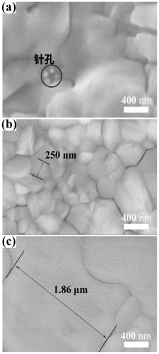
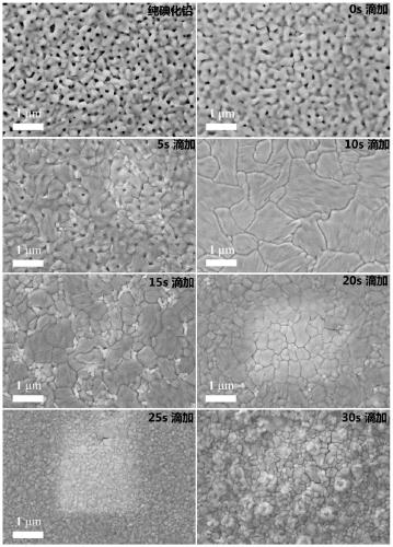
[0042] According to the steps of Example 1, the perovskite film was prepared, and the time of adding the isopropanol solution of MAI was set as: after spin coating 0s, 5s, 15s, 20s, 25s, and 30s, the isopropanol of methyl iodide was added dropwise solution. The SEM of the perovskite film that embodiment 2 obtains is as figure 2 shown.


PUM


Abstract

In a method for preparing perovskite thin films based on anti-solvent dynamic spin coating proposed by the present invention, an organic solvent that can dissolve lead iodide is selected, and an organic solvent that does not dissolve perovskite materials but is miscible with lead iodide solvents and Can dissolve CH 3 NH 3 The solvent of I (MAI) is as anti-solvent (as Virahol); In the process of spin-coating the DMF solution of lead iodide, drip the Virahol solution of MAI, by controlling the dripping amount of the Virahol solution of MAI and The timing of dropping can control the crystallization state of the perovskite film, and finally obtain a high-quality perovskite film. The surface of the perovskite thin film grown on the rough mesoporous substrate by the method of the present invention is flat and dense, without pinholes, and the grain size can reach several microns, which greatly reduces the loss of carriers at the grain boundary and is beneficial to calcium The application of titanium ore materials in the field of optoelectronics.

Description

technical field [0001] The invention relates to a method for preparing a perovskite film, in particular to a method for preparing a perovskite film based on anti-solvent dynamic spin coating. Background technique [0002] Organic-inorganic hybrid perovskite materials (CH 3 NH 3 PBX 3 ,X=Cl,Br,I), as an emerging photovoltaic semiconductor material, has excellent optoelectronic properties such as direct band gap, high light absorption coefficient, high carrier mobility and free path. Since Japanese scientist Miyasaka first applied organic-inorganic composite halide perovskite materials to the field of optoelectronics in 2009, this type of new optoelectronic materials has gradually entered the field of vision of researchers and has ushered in the peak of attention in recent years. In particular, the conversion efficiency of perovskite-based solar cells based on this material was refreshed to 23% in 2018, surpassing the current commercialized single-crystal silicon-based sola...

Claims


Application Information

Patent Timeline
Patent Type & Authority Patents(China)
IPC IPC(8): H01L51/48
CPCH10K71/15H10K71/12Y02E10/549
Inventor 熊杰孙浩轩杜新川晏超贻邬春阳戴丽萍
Owner UNIV OF ELECTRONICS SCI & TECH OF CHINA
Why Eureka
Try Eureka