Forming method for image sensor

A technology of image sensor and pixel array, which is applied in printing image acquisition, instrument, character and pattern recognition, etc., can solve problems such as difficult to improve integration and large module thickness, so as to improve production yield, increase yield, reduce Effect of Yield Loss

A technology of image sensor and pixel array, which is applied in printing image acquisition, instrument, character and pattern recognition, etc., can solve problems such as difficult to improve integration and large module thickness, so as to improve production yield, increase yield, reduce Effect of Yield Loss

CN108734071AInactive Publication Date: 2018-11-02SHANGHAI OXI TECH

Image

  • Forming method for image sensor
  • Forming method for image sensor
  • Forming method for image sensor

Examples


Embodiment Construction

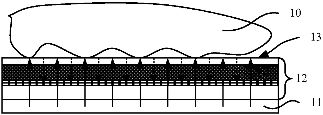
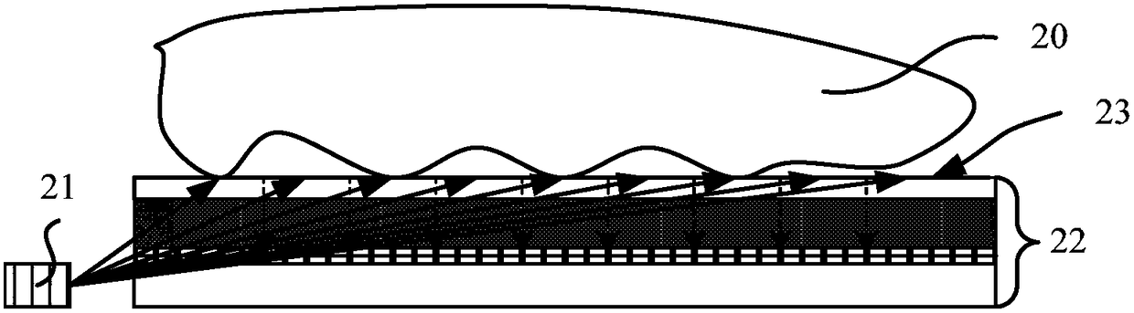
[0032] It can be seen from the background art that the fingerprint imaging module in the prior art has the problem of excessive thickness of the module. Combining with the structure of a fingerprint imaging module, the reason for the excessive thickness of the module is analyzed:

[0033] The optical fingerprint imaging module mainly includes: protective cover, optical sensor, integrated chip (IC), flexible circuit board (FPC) and electronic devices on the flexible circuit board (including light source LED), light guide plate, upper protective shell and Lower protective shell and other main components. Among them, the optical sensor is made on a glass substrate using semiconductor technology such as amorphous silicon thin film transistor (a-Si TFT), low temperature polysilicon thin film transistor (LTPS TFT) or oxide semiconductor thin film transistor (OS TFT); after cutting , dispensing, bonding and other processes to achieve packaging.

[0034] refer to figure 1 , shows a...


PUM


Abstract

The invention discloses a forming method for an image sensor. The method comprises the following steps of providing a laminated substrate, wherein the laminated substrate comprises a supporting layerand a base layer arranged on the supporting layer; forming a pixel array on the base layer; forming a protection layer on the pixel array; and removing the supporting layer to obtain the image sensor.According to the technical scheme, the thickness of the formed image sensor can be effectively reduced, so that the thickness of a fingerprint imaging module can be reduced.

Description

technical field [0001] The invention relates to the field of fingerprint imaging, in particular to a method for forming an image sensor. Background technique [0002] The fingerprint identification technology collects the fingerprint image of the human body through the fingerprint imaging module, and then compares it with the existing fingerprint imaging information in the fingerprint identification system to realize identity identification. Due to the convenience of use and the uniqueness of human fingerprints, fingerprint recognition technology has been widely used in various fields, such as: public security bureaus, customs and other security inspection fields, building access control systems, and consumer products such as personal computers and mobile phones, etc. [0003] The imaging methods of the imaging module used in the fingerprint identification technology include optical, capacitive, ultrasonic and other technologies. One of them is to collect the fingerprint im...

Claims


Application Information

Patent Timeline
02 Nov 2018
Publication
CN108734071A
IPC
G06K9/00
CPC
G06V40/1324; G06V40/1318
Inventors
曲志刚; 朱虹