LED epitaxial structure based on graphene substrate, growing method and LED

A technology of epitaxial structure and growth method, which is applied in the direction of electrical components, circuits, semiconductor devices, etc., can solve the problems of large lattice mismatch and difficult LED epitaxial structure, and achieve the effects of reducing stress, reducing bending, and high crystal quality

Active Publication Date: 2018-11-06
YANGZHOU CHANGELIGHT
View PDF6 Cites 10 Cited by
  • Summary
  • Abstract
  • Description
  • Claims
  • Application Information

AI Technical Summary

Problems solved by technology

However, it is relatively difficult to grow LED epitaxial structures on graphene substrates, mainly due to the large lattice mismatch between graphene and LED epitaxial structures.

Method used


Image

  • LED epitaxial structure based on graphene substrate, growing method and LED
  • LED epitaxial structure based on graphene substrate, growing method and LED
  • LED epitaxial structure based on graphene substrate, growing method and LED

Examples


Embodiment Construction

[0037] The following will clearly and completely describe the technical solutions in the embodiments of the present invention with reference to the accompanying drawings in the embodiments of the present invention. Obviously, the described embodiments are only some, not all, embodiments of the present invention. Based on the embodiments of the present invention, all other embodiments obtained by persons of ordinary skill in the art without making creative efforts belong to the protection scope of the present invention.

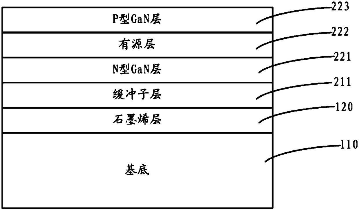
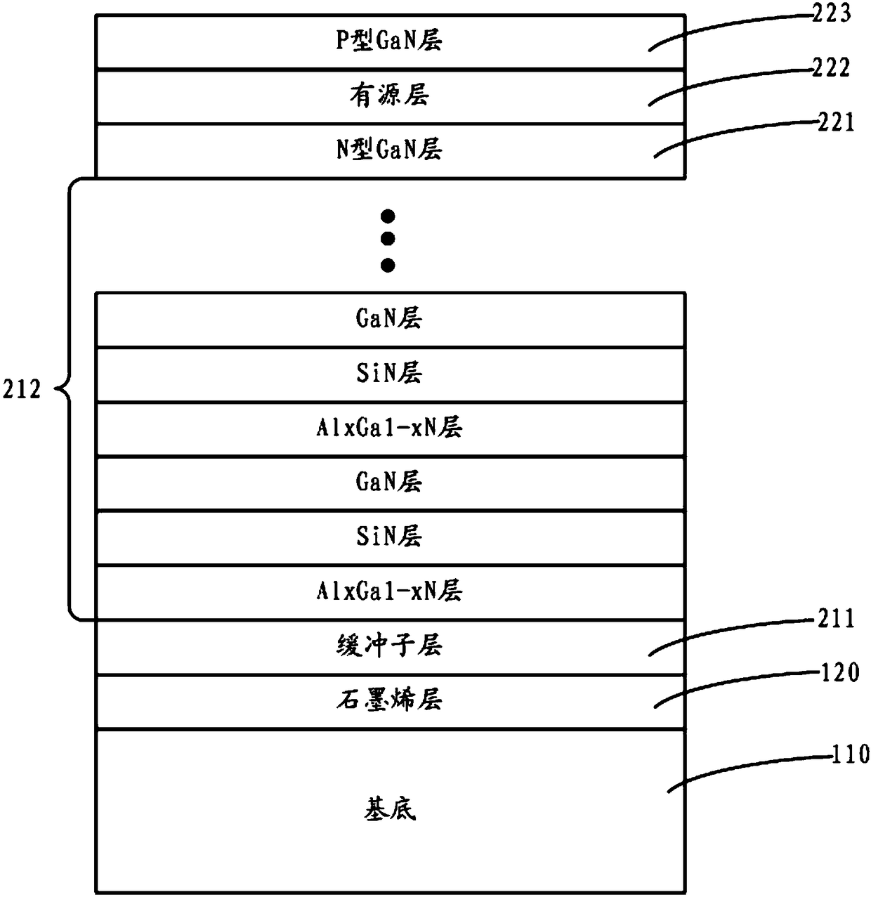
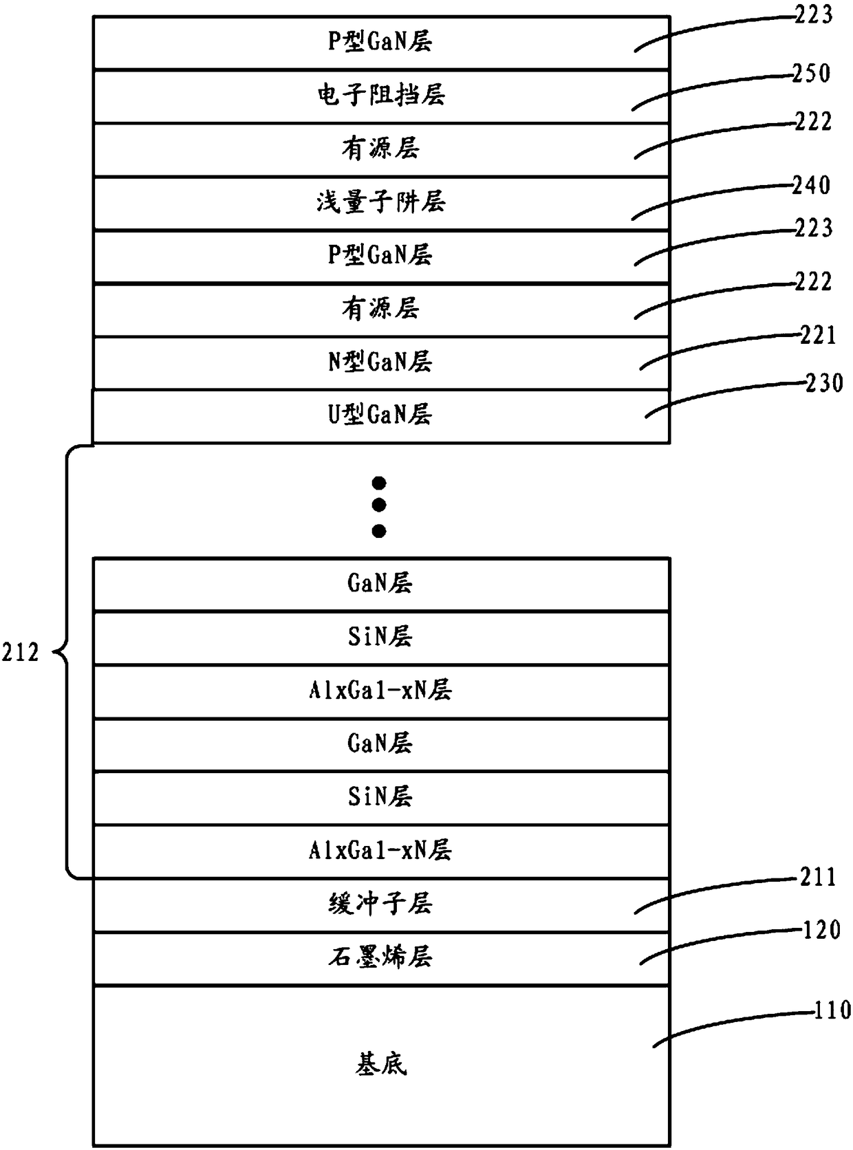
[0038] As mentioned in the background technology, as blue GaN-based LEDs are more and more widely used, people pay more attention to the brightness of blue GaN-based LEDs. Existing blue GaN-based LEDs usually grow GaN materials directly on sapphire substrates, but due to sapphire The substrate is an insulating material, so the vertical structure cannot be made directly, but it can only be peeled off, and the peeling off is very difficult, which makes the manufa...


PUM

PropertyMeasurementUnit
thicknessaaaaaaaaaa
thicknessaaaaaaaaaa
pressureaaaaaaaaaa

Abstract

The invention discloses an LED epitaxial structure based on a graphene substrate, a growing method and an LED. The graphene substrate comprises a substrate and a graphene layer positioned on the surface of one side of the substrate. The LED epitaxial structure comprises a buffer layer grown on the graphene substrate and an N-type GaN layer, an active layer and a P-type GaN layer which are grown onthe buffer layer in an overlapped manner in sequence, wherein the buffer layer comprises buffer sub-layers grown on the surface of the side, away from the substrate, of the graphene layer; the buffersub-layers are AlN buffer sub-layers, GaN buffer sub-layers, InGaN buffer sub-layers or AlGaInN buffer sub-layers. Through the technical scheme provided by the invention, the buffer layer of the LEDepitaxial structure is grown on the graphene substrate, the lattice mismatch between the LED epitaxial structure and the graphene substrate is reduced, the stress between the graphene substrate and the LED epitaxial structure is reduced, and then the LED epitaxial structure with high crystalline quality can be prepared, so that a polarization electric field is reduced effectively, the bending of an energy band is reduced, and the composite efficiency of electrons and holes is improved.

Description

technical field [0001] The invention relates to the technical field of semiconductor optoelectronic devices, more specifically, to a graphene substrate-based LED epitaxial structure and growth method and LED. Background technique [0002] Light Emitting Diode (English: Light Emitting Diode, referred to as: LED) is a very influential new product in the emerging industry of information optoelectronics. It has the advantages of small size, colorful colors, low energy consumption, and long service life. It is widely used in lighting, Display screens, signal lights, backlights, toys and other fields. Among them, light-emitting diodes represented by GaN are low in cost, and their epitaxy and chip processes are relatively mature, and they are still leading the cutting-edge and hot technologies. [0003] With the increasing application of blue GaN-based LEDs, people pay more attention to the brightness of blue GaN-based LEDs. The existing blue GaN-based LEDs usually grow GaN materi...

Claims


Application Information

Patent Timeline
Patent Type & Authority Applications(China)
IPC IPC(8): H01L33/12H01L33/32H01L33/02H01L33/00
CPCH01L33/0075H01L33/02H01L33/12H01L33/32
Inventor 田宇颜慧韩效亚杜石磊
Owner YANGZHOU CHANGELIGHT
Why Eureka
Try Eureka