Sputtering target capable of stabilizing ignition
A sputtering target and sputtering surface technology, which is applied in the field of sputtering targets, can solve the problems of undisclosed plasma pressing conditions, structures, target characteristics, etc., and achieve the effects of shortening downtime, improving cost performance, and improving production capacity
- Summary
- Abstract
- Description
- Claims
- Application Information
AI Technical Summary
Problems solved by technology
Method used
Image
Examples
Embodiment 1
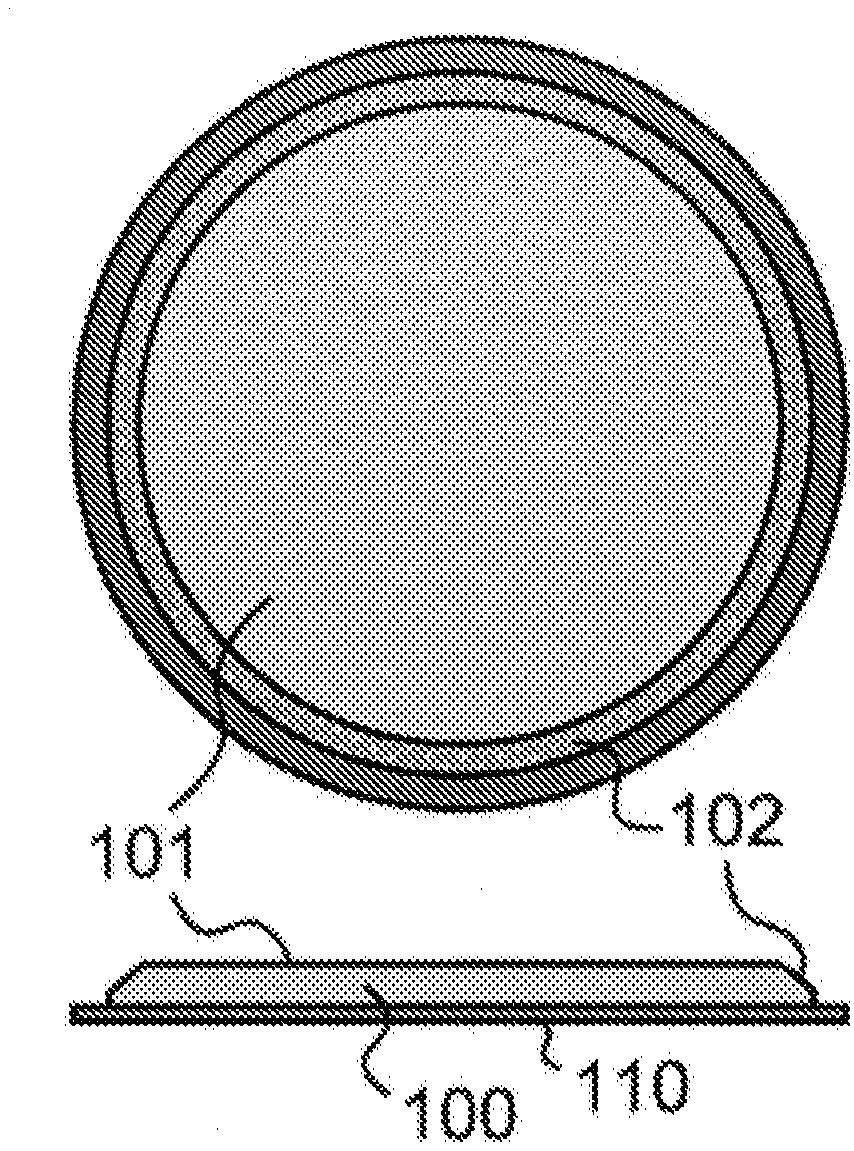
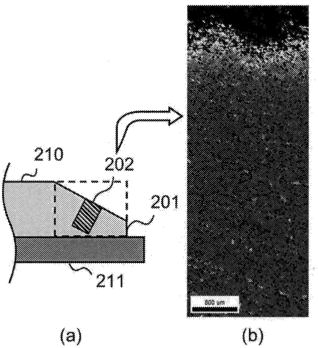
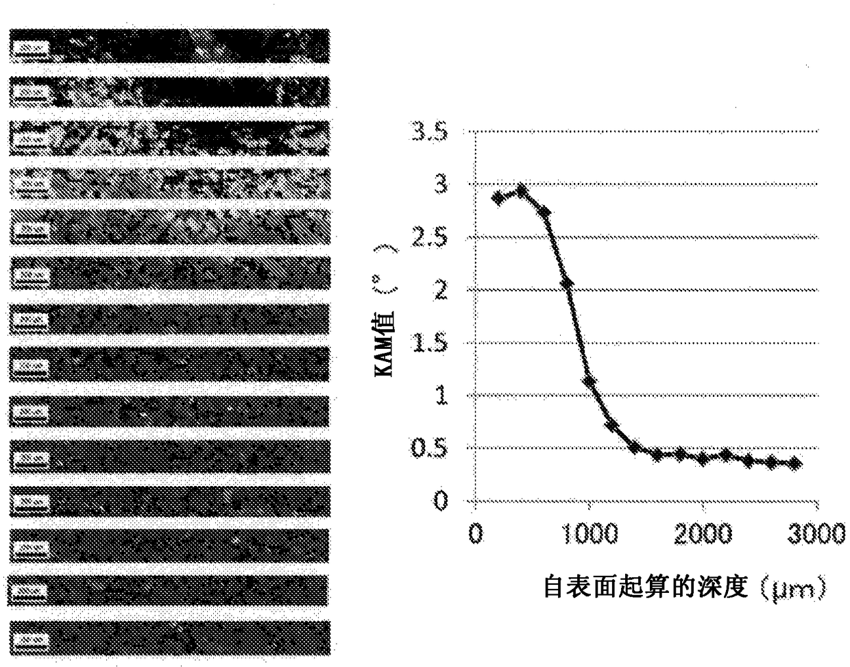
[0078] In a tantalum sputtering target having a diameter of 444 mm and a diameter of the sputtering surface of 406 mm produced in the same manner as in Comparative Example 1, the taper portion on the outer periphery of the sputtering surface was pressed with a pressing force of 1.0 mm to have an apex angle of 90°, Knurling of the knurled shaped presser at 2mm pitch, thereby introducing intentional crystalline strain in the tapered portion of the sputtering target. A photograph of the target is shown in Figure 4 (The left is the overall view, and the right is the enlarged view of the tapered part). A grid shape is formed in the tapered portion by this pressing process. Then, a sample for EBSD measurement and KAM value evaluation was prepared from the tapered portion. The sample used for EBSD measurement to evaluate the KAM value is appropriately mirror-polished and chemically etched on the surface through the surface treatment process of the above-mentioned KAM value evaluat...
Embodiment 2
[0081] In a tantalum sputtering target (purity of 4N5 or more) with a diameter of 444 mm and a diameter of the sputtering surface of 406 mm produced in the same manner as in Comparative Example 1, pressing with a pressing force of 0.5 mm has The knurling of the knurl-shaped presser with a vertex angle of 90° and a pitch of 1 mm thereby introduces intentional crystallographic strain into the tapered portion of the sputtering target. A lattice shape is formed in the tapered portion by this press working. Regarding the crystal strain of the cross-section of the tapered part, the KAM value analysis was performed by setting the maximum KAM value to 5° in units of 200 μm in the vertical direction and 1200 μm in the horizontal direction using EBSD in the same manner as in Example 1. As a result, it is an effective crystal in the present invention. The area with an average KAM value of 0.5° or more set by the amount of strain is the area from the surface to a depth of 0.8mm (4 unit ar...
Embodiment 3
[0083] In a tantalum sputtering target (purity of 4N5 or higher) with a diameter of 444 mm and a sputtering surface diameter of 406 mm produced in the same manner as in Comparative Example 1, the tapered portion on the outer periphery of the sputtering surface was formed in a concentric cross-section by lathe processing. V-shaped processing groove. At this time, the workpiece rotation speed is 200rev / min, and the cutting depth is 0.5mm / rev. The width of the groove is set to 2mm, the depth is set to 2mm, and the length of the groove is set to about 1294mm on the outer circumference and about 1281mm on the inner circumference. The lathe process of , thereby introducing intentional crystallographic strain in the tapered portion of the sputter target. Regarding the crystal strain of the cross-section of the tapered part, the KAM value analysis was performed by setting the maximum KAM value to 5° in units of 200 μm in the vertical direction and 1200 μm in the horizontal direction u...
PUM
| Property | Measurement | Unit |
|---|---|---|
| width | aaaaa | aaaaa |
| width | aaaaa | aaaaa |
Abstract
Description
Claims
Application Information


