
Display chip for virtual reality

A display chip and virtual reality technology, applied in the field of virtual reality, can solve the problems of poor comprehensive effect of display chips, poor near-eye display effect, inconvenient portability, etc., to enhance immersive experience, realize large-scale mass production, and improve standby time the effect of time

Inactive Publication Date: 2018-11-13
NANJING XUANSHI QIYUAN SOFTWARE TECH CO LTD
View PDF3 Cites 1 Cited by
  • Summary
  • Abstract
  • Description
  • Claims
  • Application Information

AI Technical Summary

Problems solved by technology

The overall effect of traditional display chips used for virtual reality is poor, which is mainly reflected in: 1. The chip is large and bulky, and it is inconvenient to carry; 2. Low resolution, poor definition, and poor near-eye display effect; 3. High cost

Method used


Image

  • Display chip for virtual reality

Examples


Embodiment 1

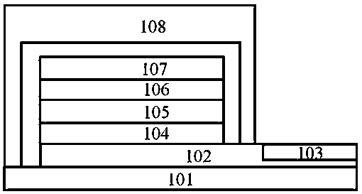
[0025] refer to figure 1 , a display chip for virtual reality, comprising: a single crystal silicon substrate 101 and a driving circuit layer 102, a bonding pad layer 103 located on the surface of the driving circuit layer 102, a cathode pixel layer 104, a color light emitting Layer 105, a transparent common anode layer 106, a single-layer thin film encapsulation layer 107, and a glass cover 108; the size of the single crystal silicon substrate 101 is 0.6 inches; the driving circuit layer 102 is made by CMOS integrated circuit technology, and its transistor The feature size is 90 nm, supporting dual voltage or multi-voltage regions, the analog circuit voltage range is -5V to +5V, and the digital circuit voltage is +1V to +5V; the driving circuit layer 102 includes a transistor layer, a transistor to metal wiring The connection hole layer of the layer, one or more metal wiring layers, one or more via layers between the metal wiring layers, a via hole under the cathode pixel lay...

Embodiment 2

[0027] refer to figure 1, a display chip for virtual reality, comprising: a single crystal silicon substrate 101 and a driving circuit layer 102, a bonding pad layer 103 located on the surface of the driving circuit layer 102, a cathode pixel layer 104, a color light emitting Layer 105, a transparent common anode layer 106, a single-layer thin film encapsulation layer 107, and a glass cover 108; the size of the monocrystalline silicon substrate 101 is less than 1 inch; the driving circuit layer 102 is made by CMOS integrated circuit technology, and its The characteristic size of the transistor is 0.13 microns, and it supports dual voltage or multi-voltage regions. The voltage range of the analog circuit is -5V to +5V, and the voltage of the digital circuit is +1V to +5V; the driving circuit layer 102 includes a transistor layer, a transistor-to-metal connection The connection hole layer of the wiring layer, one or more metal wiring layers, the via layer between one or more met...

Embodiment 3

[0029] refer to figure 1 , a display chip for virtual reality, comprising: a single crystal silicon substrate 101 and a driving circuit layer 102, a bonding pad layer 103 located on the surface of the driving circuit layer 102, a cathode pixel layer 104, a color light emitting Layer 105, a transparent common anode layer 106, a single-layer thin film encapsulation layer 107, and a glass cover 108; the size of the monocrystalline silicon substrate 101 is less than 1 inch; the driving circuit layer 102 is made by CMOS integrated circuit technology, and its The characteristic size of the transistor is 0.35 microns, supporting dual voltage or multi-voltage regions, the voltage range of the analog circuit is -5V to +5V, and the voltage of the digital circuit is +1V to +5V; the driving circuit layer 102 includes a transistor layer, a transistor to metal connection The connection hole layer of the wiring layer, one or more metal wiring layers, the via layer between one or more metal w...


PUM


Abstract

The invention relates to the technical field of virtual reality, in particular to a display chip for virtual reality. The display chip for virtual reality comprises a monocrystalline silicon substrate(101), a driving circuit layer (102), a bonding area layer (103) located on the surface of the driving circuit layer (102), a negative electrode pixel layer (104), a color light emitting layer (105),a transparent co-positive-electrode layer (106), a single-layer thin film encapsulation layer (107), and a glass packaging cover (108). According to the display chip for the virtual reality disclosedin the invention, monocrystalline silicon is adopted as a substrate, so that the size of the chip is smaller than 1 inch, integration of the display chip and a virtual reality terminal is facilitated, carrying is convenient, and miniaturization and light weight of virtual reality equipment are realized conveniently.

Description

technical field [0001] The invention relates to the technical field of virtual reality, in particular to a display chip for virtual reality. Background technique [0002] Virtual reality technology (Virtual reality referred to as VR) is to use computer graphics, electromechanical technology, electronic technology and other technologies to construct a model that simulates reality and interact with humans and computers to generate the same feedback information as in the real world, so that people can get the same experience as the real world. in the same feeling. The research on this technology began in the 1960s. Because the technology is difficult, involves a wide range, and requires high computer performance, it was first used in military aircraft flight simulation and nuclear reaction research. With the rapid development of display technology, high-speed graphics acceleration processing technology, multimedia technology, tracking system technology, etc., as well as the de...

Claims


Application Information

Patent Timeline
Patent Type & Authority Applications(China)
IPC IPC(8): H01L27/32G09G3/3225
CPCG09G3/3225H10K59/12
Inventor 邵蓉
Owner NANJING XUANSHI QIYUAN SOFTWARE TECH CO LTD
Learn More