Three-layer heterojunction organic field-effect transistor memory and fabrication method thereof

A heterojunction and organic field technology, which is applied in semiconductor/solid-state device manufacturing, electric solid-state devices, semiconductor devices, etc., can solve problems such as poor data stability, low current switch ratio, difficult multi-level storage, etc., to achieve easy operation, Effect of reducing dependence on operating voltage and improving memory speed

Inactive Publication Date: 2018-11-16
NANJING UNIV OF POSTS & TELECOMM
View PDF6 Cites 10 Cited by
  • Summary
  • Abstract
  • Description
  • Claims
  • Application Information

AI Technical Summary

Problems solved by technology

[0004] Judging from the overall research progress at home and abroad, OHTM still faces the following challenges: (1) The current research is still mainly focused on the storage phenomenon and storage behavior of OHTM, and the heterojunction organic semiconductor layer is only used as a charge transport layer. However, there are few studies on charge trapping properties in organic semiconductor layers; (2) the operating voltage is too high (>120 V), the storage speed is low (storage time>1s), the storage density is low (difficult to achieve multi-level storage), and the current switching ratio is relatively low. Low (5 s); (3) The electrical storage mechanism without adding light needs to be further elucidated and systematically explored

Method used


Image

  • Three-layer heterojunction organic field-effect transistor memory and fabrication method thereof
  • Three-layer heterojunction organic field-effect transistor memory and fabrication method thereof
  • Three-layer heterojunction organic field-effect transistor memory and fabrication method thereof

Examples


preparation example Construction

[0045] A method for preparing a three-layer heterojunction organic field effect transistor memory, comprising the following steps:

[0046] (1) Configure polymer solution, dissolve in low boiling point solvent, concentration 3~5 mg / mL;

[0047] (2) Select a suitable substrate, and sequentially form a gate electrode and a gate insulating layer on the substrate, as the substrate, the thickness of the gate insulating layer is 50~300 nm, then clean the substrate and dry it, and set it aside;

[0048] (3) Treat the dried substrate in step (2) with ultraviolet ozone for 3-5 minutes;

[0049] (4) Spin-coat the solution prepared in step (1) on the substrate prepared in step (3), with a thickness of 25-70 nm, and dry and anneal the spin-coated sample;

[0050] (5) An organic heterojunction semiconductor layer and source-drain electrodes are sequentially vapor-deposited on the sample prepared in step (4).

[0051] In step (1), the polymer in the polymer solution is polyvinylpyrrolidon...

Embodiment 1

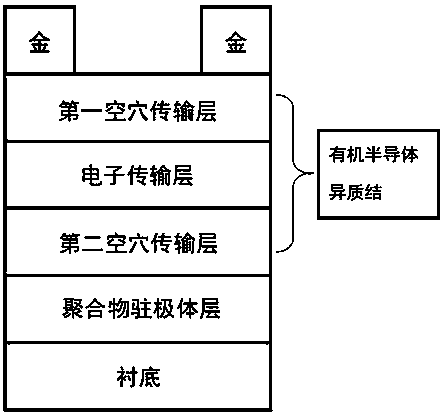
[0055] like Figure 1-8 As shown, a three-layer heterojunction organic field effect transistor memory, including:

[0056] Substrate;

[0057] a gate electrode formed over the substrate;

[0058] a gate insulating layer and a polymer electret layer covering the gate electrode, and a gate insulating layer between the gate electrode and the polymer electret layer;

[0059] a second hole transport layer formed over the polymer electret layer;

[0060] a charge transport layer formed on the second hole transport layer;

[0061] a first hole transport layer formed on the charge transport layer;

[0062] Porous source and drain electrodes formed on both sides of the channel region on the surface of the first hole transport layer.

[0063] The substrate is highly doped silicon.

[0064] In the technical solution of this embodiment 1, the materials selected for the substrate and the gate electrode are highly doped silicon, the thickness of the gate insulating layer is 50-300 nm,...

Embodiment 2

[0078] A three-layer heterojunction organic field effect transistor memory, comprising:

[0079] Substrate;

[0080] a gate electrode formed over the substrate;

[0081] a gate insulating layer and a polymer electret layer covering the gate electrode, and a gate insulating layer between the gate electrode and the polymer electret layer;

[0082] a second hole transport layer formed over the polymer electret layer;

[0083] a charge transport layer formed on the second hole transport layer;

[0084] a first hole transport layer formed on the charge transport layer;

[0085] The source and drain electrodes are formed on both sides of the channel region on the surface of the first hole transport layer.

[0086] The substrate is any one of highly doped silicon wafer, glass wafer or plastic PET.

[0087] In the technical scheme of this embodiment 2, highly doped silicon is used as the substrate and the gate electrode; a layer of 50nm silicon dioxide is used as the gate insulat...


PUM


Abstract

The invention discloses a three-layer heterojunction organic field-effect transistor memory and a fabrication method thereof. The memory comprises a substrate, wherein a source-drain electrode, an organic semiconductor heterojunction, a gate insulation layer and a gate electrode are sequentially arranged on the substrate from top to bottom, a polymer electret layer is arranged between the organicsemiconductor heterojunction and the gate insulation layer, the gate insulation layer covers a surface of the whole gate electrode and is used for isolating contact between the gate electrode and thepolymer electret layer, and the organic semiconductor heterojunction sequentially comprises a first hole transmission layer, an electron transmission layer and a second hole transmission layer from top to bottom. In the three-layer heterojunction organic field-effect transistor memory and the fabrication method thereof, provided by the invention, the polymer electret layer is fabricated on the gate insulation layer by a spinning method, morphology growth of the semiconductor heterojunction and the metal source-drain electrode is facilitated, the process is simple, the storage capacity, the current switch ratio and the storage speed can be greatly improved, the device fabrication cost is reduced, and promotion and application are convenient.

Description

technical field [0001] The invention belongs to the technical field of memory in the semiconductor transistor industry, and in particular relates to a three-layer heterojunction organic field-effect transistor memory and a preparation method thereof. Background technique [0002] As a basic component in electronic circuits, organic field-effect transistors can be applied to large-area printing processes because of their wide source of materials, softness, and simple processing technology. They are very suitable for the development direction of the next-generation wearable electronics industry. The structure of the effect transistor determines that it has a wealth of functional applications, such as light emission, storage, sensing, switching, etc., so it has broad application prospects in the field of information electronics. [0003] Heterojunction organic field-effect transistor electrical memory (OHTM) is an integrated device of organic field-effect transistor memory (OFE...

Claims


Application Information

Patent Timeline
Patent Type & Authority Applications(China)
IPC IPC(8): H01L51/05H01L51/10H01L51/40
CPCH10K10/486H10K10/84H10K10/466
Inventor 仪明东宋子忆李雯李宇陈旭东李焕群
Owner NANJING UNIV OF POSTS & TELECOMM
Why Eureka
Try Eureka