ZnO composite transparent conductive thin film based on flexible substrate and preparation method thereof
A technology of transparent conductive film and flexible substrate, which is applied to conductive layers on insulating carriers, cable/conductor manufacturing, circuits, etc., can solve the problems of unfavorable transparent conductive film light transmittance, affecting the performance of final products, and high film cost. To meet the requirements of industrial production, to facilitate large-scale industrial preparation, and to achieve good repeatability
- Summary
- Abstract
- Description
- Claims
- Application Information
AI Technical Summary
Problems solved by technology
Method used
Image
Examples
Embodiment 1
[0029] Choose flexible PET as the substrate, cut the raw material PET into square pieces with an area of 15 mm×15 mm, put the flexible PET substrate into deionized water and absolute ethanol for 10 min, and then take it out with a nitrogen gun Dry and set aside; place the flexible PET substrate on the sample stage of the magnetron sputtering coating apparatus, adjust the distance between the sample stage and the target to be 53 cm, replace the ZnO target (the purity of the ZnO target is 99.99%), cover and Tighten the bleed valve of the flange cover, turn on the vacuum pump switch and start the vacuum system to start pumping the air in the chamber. When the vacuum reaches 1 Pa or below, inject pure argon Ar (purity 99.999%) for about 5 minutes; The RF power is turned on, the sputtering power is adjusted to 100W, the sputtering pressure is 15 Pa, and the rotation speed of the sample stage is 12 r / min. After 2 minutes of pre-sputtering, the stopper is removed to deposit a bottom...
Embodiment 2
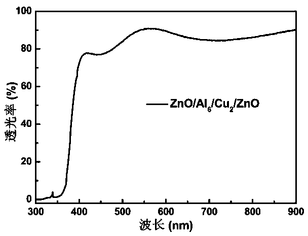
[0035] The bottom ZnO is the same as in Example 1, except that after sputtering the bottom ZnO, an Al target (the purity of the Al target is 99.995%) is replaced, the sputtering power is adjusted to 150W, the sputtering pressure is 15 Pa, and the sample stage speed is 4 r / min , after pre-sputtering, Al with a thickness of 6 nm was deposited on the surface of the bottom ZnO; in the same way, a Cu target was replaced (the purity of the Cu target was 99.995%), and the sputtering power was adjusted to 30W, the sputtering pressure was 15Pa, and the speed of the sample stage was 4 r / min, deposit Cu with a thickness of 2 nm on the surface of the Al layer after pre-sputtering; finally replace the ZnO target, adjust the sputtering power to 100W, sputtering pressure 15 Pa, sample stage speed 12 r / min, pre-sputtering Finally, a top layer of ZnO with a thickness of 50 nm is deposited on the surface of the Cu layer to obtain a flexible substrate-based ZnO / Cu 2 / Al 6 / ZnO composite transp...
Embodiment 3
[0039] The bottom ZnO is the same as in Example 1, the difference is that after sputtering the bottom ZnO, the Cu target (the purity of the Cu target is 99.995%) is replaced, the sputtering power is adjusted to 30W, the sputtering pressure is 15 Pa, and the speed of the sample stage is 4 r / min , after pre-sputtering, Cu with a thickness of 4 nm was deposited on the surface of the bottom ZnO; similarly, an Al target was replaced (the purity of the Al target was 99.995%), and the sputtering power was adjusted to 150W, the sputtering pressure was 15Pa, and the speed of the sample stage was 4 r / min, after pre-sputtering, deposit Al with a thickness of 4 nm on the surface of the Cu layer; finally replace the ZnO target, adjust the sputtering power to 100W, sputtering pressure 15 Pa, sample stage speed 12 r / min, pre-sputtering Then deposit a top layer of ZnO with a thickness of 50 nm on the surface of the Cu layer to obtain a flexible substrate-based ZnO / Al 4 / Cu 4 / ZnO composite ...
PUM
| Property | Measurement | Unit |
|---|---|---|
| Thickness | aaaaa | aaaaa |
| Thickness | aaaaa | aaaaa |
| Sheet resistance | aaaaa | aaaaa |
Abstract
Description
Claims
Application Information
 - R&D
- Intellectual Property
- Life Sciences
- Materials
- Tech Scout
- Unparalleled Data Quality
- Higher Quality Content
- 60% Fewer Hallucinations
Browse by: Latest US Patents, China's latest patents, Technical Efficacy Thesaurus, Application Domain, Technology Topic, Popular Technical Reports.
© 2025 PatSnap. All rights reserved.Legal|Privacy policy|Modern Slavery Act Transparency Statement|Sitemap|About US| Contact US: help@patsnap.com


