Static random access memory and fabrication method thereof
A technology of static random storage and manufacturing method, which is applied in the direction of electrical components, transistors, electric solid-state devices, etc., can solve the problems of weak anti-noise ability, large area occupied by SRAM cells, and poor stability, so as to improve anti-noise ability and suppress leakage Power consumption and transistor threshold voltage drift, the effect of convenient SRAM chip
- Summary
- Abstract
- Description
- Claims
- Application Information
AI Technical Summary
Problems solved by technology
Method used
Image
Examples
Embodiment 1
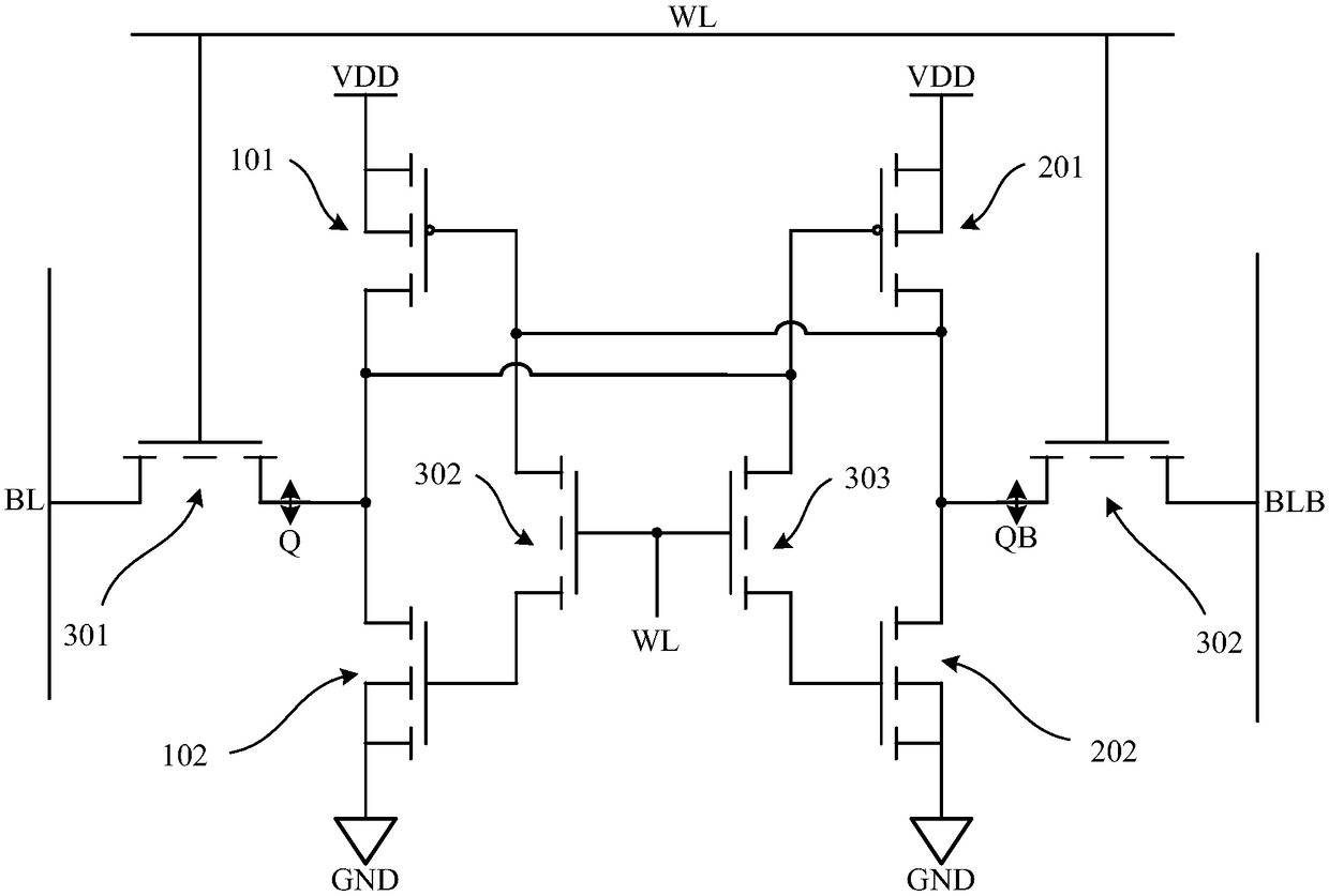
[0089] The present invention provides a static random memory unit, based on a PD SOI device with a body contact structure, and uses eight transistors, please refer to figure 1 , shown as a schematic diagram of the circuit principle of the SRAM unit, including:
[0090] The first PMOS pull-up transistor 101, the second PMOS pull-up transistor 201, the first NMOS pull-down transistor 102, the second NMOS pull-down transistor 202, the first NMOS access transistor 301, the second NMOS access transistor 302, the third NMOS memory Access pipe 303 and fourth NMOS access pipe 304 .
[0091] Specifically, the gate of the first PMOS pull-up transistor 101 is connected to the drain of the second PMOS pull-up transistor 201, and the drain of the first PMOS pull-up transistor 101 is connected to the second PMOS pull-up transistor 201. The gate of the transistor 201 is connected, and the source of the first PMOS pull-up transistor 101 and the source of the second PMOS pull-up transistor 20...
Embodiment 2
[0111] The present invention also provides a manufacturing method of a static random storage unit, comprising the following steps:
[0112] First, step 1) is performed to provide an SOI substrate including a back substrate, an insulating buried layer, and a top layer of silicon in sequence from bottom to top, and a shallow trench isolation structure is formed in the top layer of silicon to define an active region.
[0113] Specifically, such as Figure 8 As shown, four active regions 20a, 20b, 20c and 20d are defined, wherein these four active regions 20a, 20b, 20c and 20d are arranged in parallel in turn, and shallow trenches are formed around each active region, and the shallow trenches The track is filled with insulating material to form a shallow trench isolation structure. In this embodiment, the insulating material is silicon dioxide.
[0114]Then perform step 2) fabricate an N well 30, a first P well 40 and a second P well 50 in the top silicon according to the positi...
PUM
 Abstract
Description
Claims
Application Information


