Macroscopic ordered body of silicon carbide nanowires and preparation method thereof
A silicon carbide nanowire and macroscopic technology, applied in the field of nanomaterials, can solve the problem of less directional arrangement of silicon carbide nanowires, and achieve the effects of improving anisotropy, improving thermal performance, and three-dimensional scale control
- Summary
- Abstract
- Description
- Claims
- Application Information
AI Technical Summary
Problems solved by technology
Method used
Image
Examples
Embodiment 1
[0038] A method for directional arrangement of silicon carbide nanowires, the specific steps are:
[0039] (1) Using sodium dodecylsulfonate as a dispersant, controlling the mass ratio of silicon carbide nanowires to sodium dodecylsulfonate to 5:1, and the mass ratio of silicon carbide nanowires to acetone to 1:10, using ultrasonic technology Uniformly disperse the silicon carbide nanowires in acetone to obtain a disordered silicon carbide nanowire suspension, the ultrasonic power is 300W, and the ultrasonic time is 1h;
[0040] (2) Using polymethyl methacrylate as a binder and dibutyl phthalate as a plasticizer, adding a suspension of disordered silicon carbide nanowires to obtain a silicon carbide nanowire slurry. The mass ratio of polymethyl methacrylate to dibutyl phthalate is 1:1, the mass ratio of silicon carbide nanowires to binder is 5:1, the ultrasonic power is 300W, and the time is 1h;
[0041] (3) Transfer the disordered silicon carbide nanowire slurry to a casting...
Embodiment 2
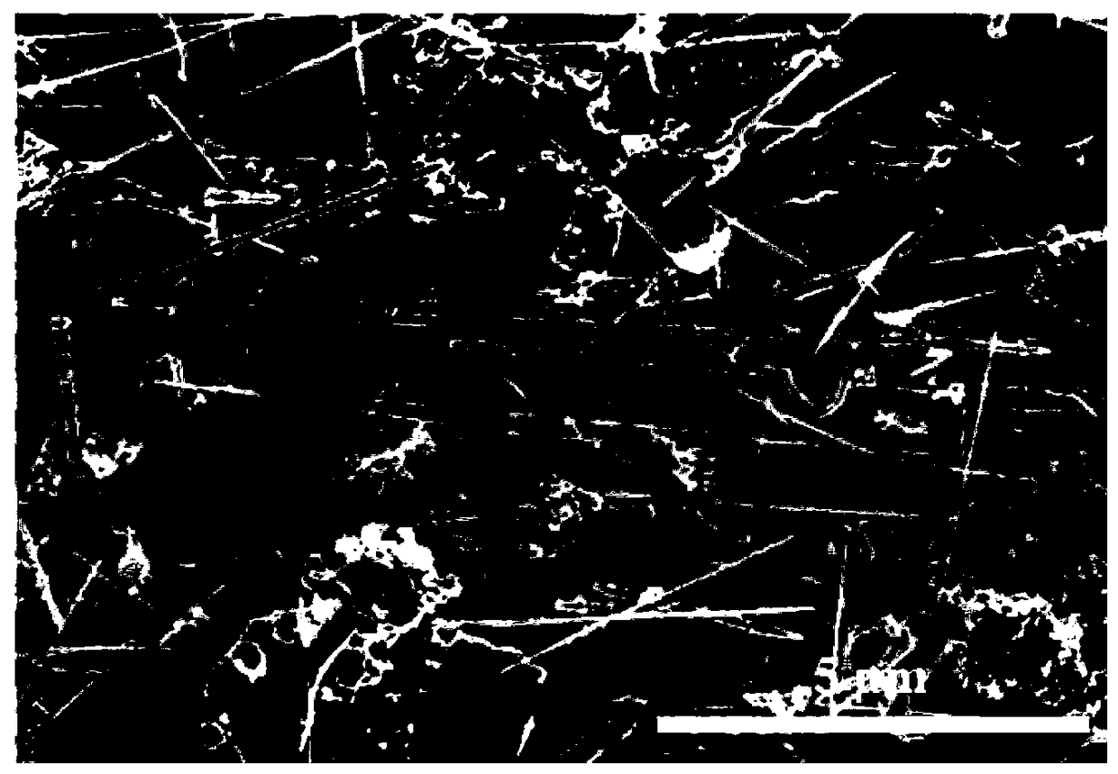
[0044] The difference between this embodiment and Example 1 is that in the (2) step of the preparation step, the ratio of the silicon carbide nanowires to the binder is controlled to be 1:1 to obtain a silicon carbide nanowire film with a higher volume content, Scanning microscope photographs such as image 3 shown.
Embodiment 3
[0046] The difference between this embodiment and embodiment 1 is: in the step (4) of the preparation step, the stretching percentage is controlled to be 80%. All the other components and preparation steps are the same as in Example 1. SiC nanowires with a greater degree of order were obtained, and the scanning microscope photos were as follows Figure 4 shown.
PUM
 Abstract
Description
Claims
Application Information


