A manufacture method for improving three-dimensional micro-nano structure base on composite scanning

A processing method and technology of micro-nano structure, applied in the photolithography process of patterned surface, microlithography exposure equipment, photolithography process exposure device, etc., can solve the problems of slow response time, difficulty in processing three-dimensional structure, and difficulty in satisfying , to achieve the effect of improving width precision, reducing width error and improving smoothness

Active Publication Date: 2018-12-11
JINAN UNIVERSITY
View PDF4 Cites 4 Cited by
  • Summary
  • Abstract
  • Description
  • Claims
  • Application Information

AI Technical Summary

Problems solved by technology

Usually, the three-dimensional piezoelectric displacement platform with nanoscale repeat positioning accuracy has a relatively large inertia and a slow response time of more than 10ms, so it takes a long time to prepare the micro-nano structure and the size error is large
Although the moment of inertia of the two-dimensional galvanometer is small and the response time is fast, the scanning of the two-dimensional galvanometer is limited to processing high-precision structures in the two-dimensional plane, and it is difficult to process complex three-dimensional structures.
Therefore, simply using the above two scanning methods to process three-dimensional micro-nano structures has been difficult to meet the rapid development of high-precision micro-nano diffractive optical device manufacturing and integrated optoelectronic devices in terms of processing time, dimensional accuracy of formed devices, and surface smoothness control. Corresponding requirements in application fields such as preparation and biomedical device processing

Method used


Image

  • A manufacture method for improving three-dimensional micro-nano structure base on composite scanning
  • A manufacture method for improving three-dimensional micro-nano structure base on composite scanning
  • A manufacture method for improving three-dimensional micro-nano structure base on composite scanning

Examples


Embodiment

[0033] This embodiment discloses a processing method for improving a three-dimensional micro-nano structure based on composite scanning, including the following steps:

[0034] S1, coating photoresist on the substrate;

[0035] S2. Adjust the optical signal emitted by the laser light source according to the exposure requirements of the photoresist, including beam expansion, polarization adjustment, phase adjustment, light intensity adjustment, etc.;

[0036] S3. Pass the adjusted laser beam through the two-dimensional vibrating mirror first, and then focus on the specified position in the photoresist through the objective lens;

[0037] S4. Split the three-dimensional structural model to be processed into several two-dimensional planes along the longitudinal axis, and each two-dimensional plane figure is filled and fitted by several points;

[0038] S5. Import the spatial coordinate information of all the points combined into the three-dimensional model structure into the pro...

Embodiment 2

[0053] In this embodiment, according to the processing method of improving the three-dimensional micro-nano structure based on compound scanning of the present invention, the specific implementation steps of preparing a structure composed of lines in the photoresist with the trade name SZ2080 are described in detail:

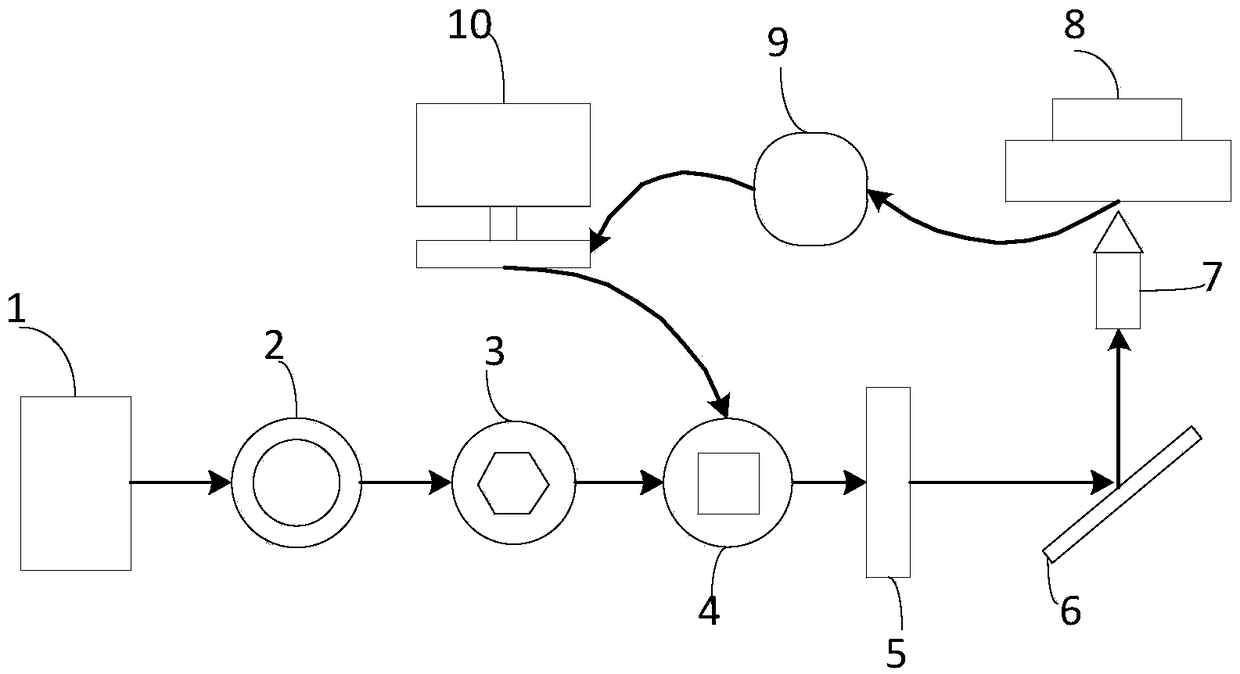
[0054] (1) The processing equipment used in this embodiment is as figure 1 As shown, the device marked 1 in the figure represents a femtosecond pulse laser, which emits laser pulses with a wavelength of 532nm. The laser beam is emitted from the laser and passes through a 1 / 2 wave plate used to adjust the light intensity, marked as 2 in the figure. Then the laser beam passes through an aperture (No. 3) and a shutter (No. 4) to reach the front of the two-dimensional vibrating mirror (No. 5). Then the laser beam passes through the vibrating mirror and enters the objective lens vertically placed under the three-dimensional platform through a reflector (No. 7). Fi...


PUM

PropertyMeasurementUnit
wavelengthaaaaaaaaaa

Abstract

The invention discloses a method for improving three-dimensional micro-nano structure based on composite scanning. The method includes such steps as coating photoresist on substrate; Adjusting the light signal emitted from the laser light source according to the exposure demand of the photoresist; passing the adjusted laser beam is firstly through a two-dimensional vibrating mirror, and then focusingon a designated position in the photoresist through an objective lens; dividing the three-dimensional structure model to be processed into a plurality of two-dimensional planes along the longitudinal axis direction; importing the spatial coordinate information of all the points which are combined into a three-dimensional model structure into the control system of the machining platform. The micro-moving platform moves under the preset motion trajectory of the control system, and the photoresist is exposed according to the motion trajectory of the platform under the irradiation of the laserbeam. While the micro-moving platform moves along the preset trajectory, the two-dimensional vibrating mirror vibrates in another vibration mode, that is, the exposure trajectory of the light spot focused in the photoresist is composed of the superposition of the two-dimensional vibrating mirror trajectory and the three-dimensional micro-nano-moving platform trajectory.

Description

technical field [0001] The invention relates to the technical field of three-dimensional micro-nano structure processing, in particular to a processing method for improving three-dimensional micro-nano structures based on composite scanning. Background technique [0002] As an important advanced manufacturing method of three-dimensional micro-nano structure, femtosecond laser processing technology has been widely used in many industrial processing and manufacturing fields. Traditionally, the method of processing materials based on a focused continuous laser beam, on the one hand, is limited by the theoretical basis of the optical diffraction limit, and the processing resolution is suppressed at the micron and submicron scales, making it difficult to process ultra-high-precision micro-nano structures at the nanoscale. On the one hand, limited by the single-photon interaction mechanism, the processed object is usually limited to a two-dimensional planar structure. In recent y...

Claims


Application Information

Patent Timeline
Patent Type & Authority Applications(China)
IPC IPC(8): G03F7/20
CPCG03F7/2053
Inventor 曹耀宇李湘滔李向平
Owner JINAN UNIVERSITY
Why Eureka
Try Eureka