A light receiving front-end circuit with feedback

A front-end circuit and light receiving technology, which is applied in the direction of negative feedback circuit layout, amplifier with field effect device, amplifier with only semiconductor devices, etc., can solve problems such as instability, low signal-to-noise ratio, incomplete image data, etc. Achieve the effect of easy implementation, small area and low power consumption

Inactive Publication Date: 2018-12-11
厦门芯豪科技有限公司
View PDF5 Cites 2 Cited by
  • Summary
  • Abstract
  • Description
  • Claims
  • Application Information

AI Technical Summary

Problems solved by technology

In the system, the small signal makes the signal-to-noise ratio low, and the signal is easily affected by various interferences, so that the output image is either distorted or unstable.
A narrower bandwidth will filter out part of the required frequency information, which will eventually make the image data incomplete

Method used


Image

  • A light receiving front-end circuit with feedback
  • A light receiving front-end circuit with feedback
  • A light receiving front-end circuit with feedback

Examples


Embodiment Construction

[0019] Specific embodiments of the present invention will be described in detail below in conjunction with the accompanying drawings.

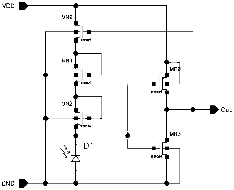
[0020] Such as figure 2 As shown, the load of the photodiode D1 of the present invention is three series-connected N-type MOS transistors (MN0, MN1, MN2). A P-type MOS transistor MP0 and an N-type MOS transistor MN3 together form an inverting amplifier, its input is the cathode of the photodiode D1, and its output is connected to the gate terminal of MN0; forming a negative feedback circuit.

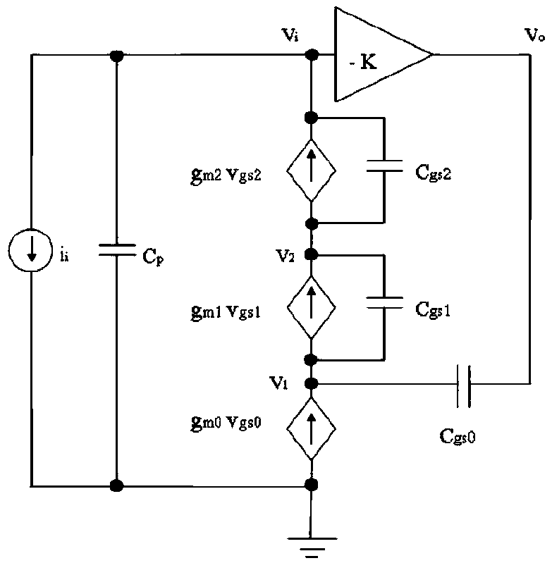
[0021] image 3 for figure 2 Small-signal equivalent circuit diagram of the circuit shown. In the figure, photodiode D1 is equivalent to a current source i i The parasitic capacitance Cp of the photodiode D1 is connected in parallel; the N-type MOS transistors MN0, MN1, and MN2 are respectively equivalent to a voltage-controlled current source and their respective parasitic capacitance Cgs; the inverter is equivalent to a magnification factor of -K...


PUM


Abstract

A light receiving front-end circuit with feedback has three N-type MOSFETs (MN0, MN1, MN2) connected in series as a load of a photodiode D1. And a P-type MOS transistor MP0 and an N-type MOS transistor MN3 together form a reverse amplifier, the input of which is the cathode of the photodiode D1, and the output of which is connected to the gate terminal of the photodiode MN0, constituting a negative feedback circuit. The invention adopts a scheme of integrating a photosensitive device and a signal conversion and amplification on an active pixel sensor (APS), and realizes the triple functions ofreceiving an optical signal, converting the optical signal into an electric signal and amplifying the optical signal through a relatively simple circuit. The light sensing circuit of the invention isrealized by a photodiode, and the amplifier is realized by a high gain circuit with feedback. These circuits have the advantages of small area, low power dissipation and easy implementation in standard CMOS process.

Description

technical field [0001] The invention relates to an integrated circuit, and in particular provides a light-receiving front-end circuit with feedback. Background technique [0002] In application fields such as laser Doppler flowmeter, in order to quickly scan a high-definition image of the detected area, we need to make the photosensitive device into a 2-dimensional array, and make each photosensitive pixel correspond to Part of the irradiated area. Therefore, for an irradiated area of ​​a certain size, we can improve the definition of the image by increasing the scale of the array, that is, increasing the number of photoreceptor pixels. [0003] The traditional laser Doppler flowmeter has low integration, and the photosensitive device and signal processing circuit are relatively independent. Although the technology is relatively mature, it is bulky and inconvenient to carry around, which limits its application. And its high cost makes it difficult for such products to be ...

Claims


Application Information

Patent Timeline
Patent Type & Authority Applications(China)
IPC IPC(8): H03F1/34H03F3/08H03F3/10H03F3/16
CPCH03F1/342H03F3/082H03F3/087H03F3/10H03F3/16
Inventor 顾全
Owner 厦门芯豪科技有限公司
Why Eureka
Try Eureka