High-stability chalcogenide microsphere on-chip coupling device

A high-stability, on-chip coupling technology, applied in the field of integrated photonic device research, can solve problems such as low loss, the impact of the actual application of microspheres at the packaging point, and the limitation of the evanescent field application of microspheres.

Inactive Publication Date: 2018-12-18
广州米德红外科技有限公司
View PDF4 Cites 0 Cited by
  • Summary
  • Abstract
  • Description
  • Claims
  • Application Information

AI Technical Summary

Problems solved by technology

[0003] The fully-wrapped packaging structure uses ultraviolet light curing glue to wrap the entire coupling system of microspheres and tapered optical fibers. The refractive index of the light curing glue used is smaller than that of microspheres and optical fibers, and the loss is small. The advantages of this structure are The whole structure is encapsulated, so it is not affected by external dust, etc., and the coupling method is fixed, so it is not easily affected by external vibrations, etc. Application of Microsphere Evanescent Field in Sensing, Biomolecular Detection and Other Fields
[0004] The point packaging technology is to fill the coupling area of ​​the microsphere and the tapered optical fiber with a glue with a lower refractive index and lower loss. Compared with the full package packaging technology, this structure does not affect the evanescent field sensing application of the microsphere cavity. , but the operation of this encapsulation technology is difficult, and the encapsulation point is too large or too small will affect the actual application of microspheres

Method used


Image

  • High-stability chalcogenide microsphere on-chip coupling device

Examples


Embodiment Construction

[0022] The specific implementation of the present invention will be further described below in conjunction with the accompanying drawings and specific embodiments. It should be pointed out that the described embodiments are only a part of the embodiments of the present invention, rather than all embodiments. Based on the embodiments of the present invention, all those skilled in the art can obtain without creative work. Other embodiments all belong to the protection scope of the present invention.

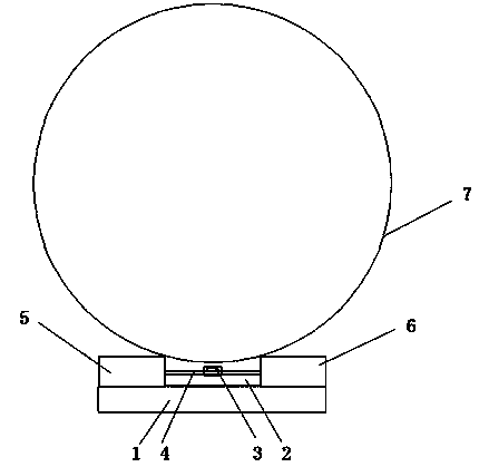
[0023] like figure 1 As shown, it is a structural schematic diagram of a highly stable chalcogenide microsphere on-chip coupling device of the present invention, including a substrate layer 1, a lower cladding layer 2, a ridge-shaped optical waveguide 3, a dielectric layer 4, and a first polymer support layer 5. The second polymer support layer 6 and microspheres 7, the upper surface of the substrate layer 1 is in contact with the lower cladding layer 2, the upper surface of the l...


PUM


Abstract

The invention discloses a high-stability chalcogenide microsphere on-chip coupling device. The high-stability chalcogenide microsphere on-chip coupling device comprises a substrate layer, a lower cladding layer, a ridge optical waveguide, a dielectric layer, a first polymer support layer, a second polymer support layer and microspheres, wherein the upper surface of the substrate layer is contact connection with the lower cladding layer; the upper surface of the lower cladding layer is connected with the ridge optical waveguide; the upper surface of the ridge optical waveguide is in contact connection with the dielectric layer; the first polymer support layer and the second polymer support layer are arranged on the left and right sides of the dielectric layer respectively; the first polymersupport layer and the second polymer support layer are placed on the substrate layer; and the microspheres are placed between the two support layers in a contact manner. A high-stability chalcogenidemicrosphere on-chip coupling device disclosed by the invention is compatible with an existing CMOS process, and has the advantages of high integration degree, high stability and insusceptibility to external air disturbance.

Description

technical field [0001] The invention relates to the research field of integrated photonic devices, in particular to a highly stable chalcogenide microsphere on-chip coupling device. Background technique [0002] The optical resonant cavity can confine the light field to a small space area. The light field in this area has a high energy density and a specific light field distribution, which is very useful for studying the interaction between light and matter, developing photonic devices, and realizing light Information processing is of great significance. Optical resonators mainly include Fabry-Perot cavities, photonic crystal microcavities, and whispering gallery mode microcavities. Among them, whispering gallery mode microcavities have attracted great attention from researchers due to their high quality factor, small mode volume, and ease of preparation. It has become the most widely studied optical microcavity in the past 20 years. Typical structures in whispering galler...

Claims


Application Information

Patent Timeline
Patent Type & Authority Applications(China)
IPC IPC(8): G02B6/122G02B6/26
Inventor 熊松松
Owner 广州米德红外科技有限公司
Why Eureka
Try Eureka