Method for completely removing metal layer between wafer-level soi material and glass electrostatic bonding surface
A complete removal and electrostatic bonding technology, applied in circuits, electrical components, semiconductor devices, etc., can solve the problem that the metal layer cannot be completely removed, and achieve the effect of reducing the leakage defect rate and improving the bonding quality and bonding strength.
- Summary
- Abstract
- Description
- Claims
- Application Information
AI Technical Summary
Problems solved by technology
Method used
Image
Examples
specific Embodiment approach 1
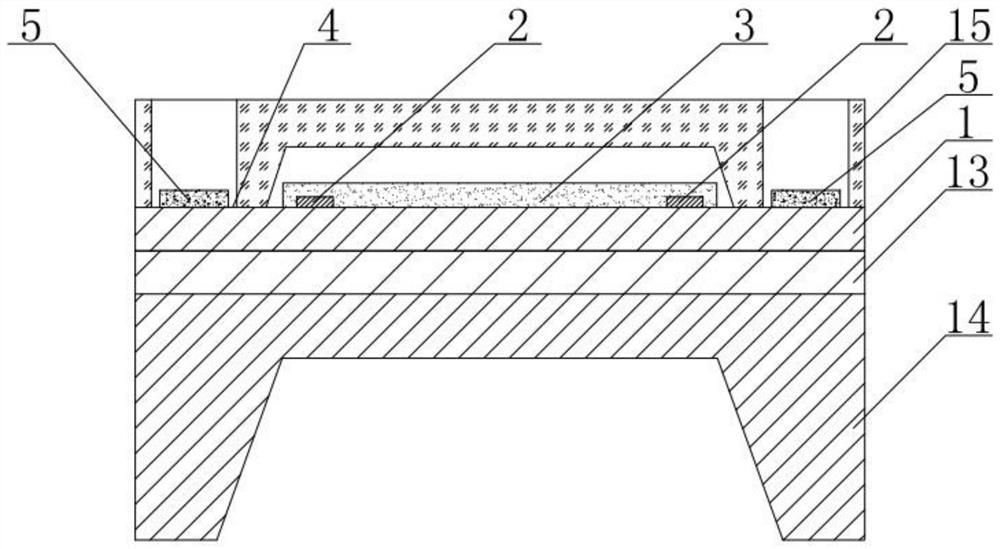
[0022] The method for completely removing the metal layer between the wafer-level SOI material and the glass electrostatic bonding surface of the present invention comprises the following steps:
[0023] Step 1: Coat the top layer of silicon 1 on the SOI silicon wafer with photoresist, perform photoetching on the photoresist according to the design requirements, and then etch the top layer of silicon 1, so that a part of the top layer of silicon 1 is etched to form a sensitive resistor 2 , and finally remove the photoresist.
[0024] Step 2: performing thermal oxidation and chemical vapor deposition on the upper surface of the top layer silicon 1 and the sensitive resistor 2 in sequence to form a composite dielectric film 3 .
[0025] The top layer silicon 1 includes the sensitive resistor 2 formed by etching and the remaining part of the top layer silicon 1 etched in step 1, and the composite dielectric film 3 formed on the sensitive resistor 2 can also be called a resistance...
specific Embodiment approach 2
[0038] The difference between the second embodiment and the first embodiment is that in the second step, thermal oxidation and chemical vapor deposition are performed on the upper surface of the top silicon 1 and the sensitive resistor 2 to form a composite dielectric film 3, specifically: first, the top silicon 1 and the upper surface of the sensitive resistor 2 are thermally oxidized to form silicon dioxide SiO 2layer, and then use low pressure chemical vapor deposition method LPCVD on SiO 2 Silicon Nitride Si 3 N 4 layer, SiO 2 layer with Si 3 N 4 layer constitutes a composite dielectric membrane.
[0039] The oxidation process can be carried out in a dry, wet or dry manner.
specific Embodiment approach 3
[0041] The difference between the third embodiment and the first embodiment is that in step 2, thermal oxidation and chemical vapor deposition are performed on the upper surface of the top layer silicon 1 and the sensitive resistor 2 to form a composite dielectric film 3, specifically: first, the top layer silicon 1 and the The upper surface of the sensitive resistor 2 is thermally oxidized to form SiO 2 layer, and then use plasma enhanced chemical vapor deposition method PECVD on SiO 2 SiO 2 / Si 3 N 4 Composite layer, SiO 2 layer with SiO 2 / Si 3 N 4 The composite layer constitutes a composite dielectric membrane. SiO 2 / Si 3 N 4 Composite layer is SiO 2 Layer plus Si 3 N 4 Composite layer composed of layers.
[0042] The oxidation process can be carried out in a dry, wet or dry manner.
PUM
 Abstract
Description
Claims
Application Information


