Manufacturing method of gate

A manufacturing method and gate technology, applied in the field of gate manufacturing, can solve problems such as photoresist 206 loss, polysilicon gate damage, and affecting component electrical properties, so as to reduce the cost of the mask and improve the consistency

Active Publication Date: 2021-02-02
SHANGHAI HUALI INTEGRATED CIRCUIT CORP
View PDF4 Cites 0 Cited by
  • Summary
  • Abstract
  • Description
  • Claims
  • Application Information

AI Technical Summary

Problems solved by technology

In the process of etching back the oxide layer 105, the photoresist 206 has a certain loss. When the oxide layer 105 on the top of some gates has not been removed, the height of part of the photoresist 206 is already lower than the height of the polysilicon gate 103. , thus exposing the sides of the polysilicon gate 103
The transition loss of the photoresist 206 caused by the excessive height difference of the gate is likely to cause damage to the active region and the polysilicon gate, which will affect the electrical properties of the component.
[0009] Additionally, by Figure 1C It can be seen that after the oxide layer 105 is etched back, the heights of the sidewalls 107 are different, and the different heights of the sidewalls 107 will lead to different etching loads of the sidewalls 107, which is not conducive to subsequent planarization.

Method used


Image

  • Manufacturing method of gate
  • Manufacturing method of gate
  • Manufacturing method of gate

Examples


Embodiment Construction

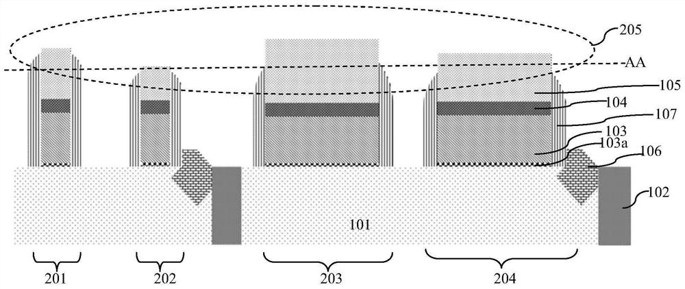
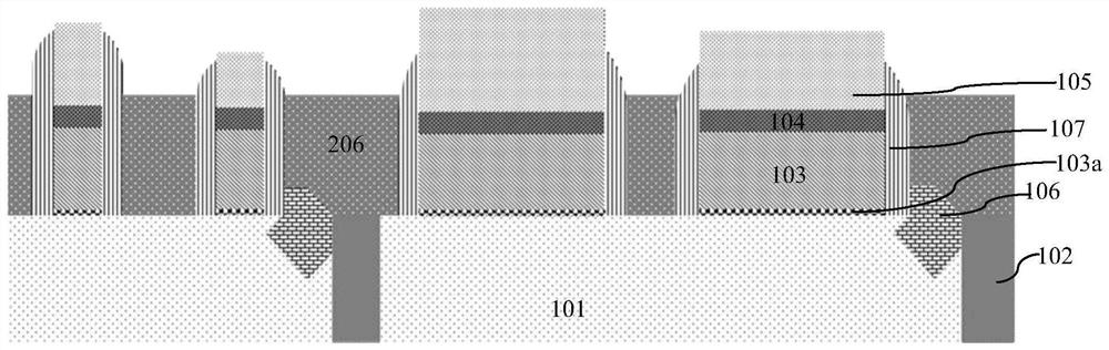
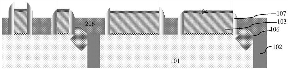
[0041] Such as figure 2 Shown is the flow chart of the method of the embodiment of the present invention; Figure 3A to Figure 3F As shown, it is a device structure diagram in each step of the method of the embodiment of the present invention. The manufacturing method of the gate of the embodiment of the present invention includes the following steps:

[0042] Step 1, such as Figure 3A As shown, a semiconductor substrate 1 is provided, and a gate dielectric layer 3 a and a polysilicon gate 3 are sequentially formed on the surface of the semiconductor substrate 1 .

[0043] In the embodiment of the present invention, the semiconductor substrate 1 is a silicon substrate.

[0044] The gate dielectric layer 3a includes a high dielectric constant layer, and there is an interface layer between the high dielectric constant layer and the semiconductor substrate 1 . The interfacial layer is usually silicon oxide.

[0045] A field oxide layer 2 is formed in the semiconductor subst...


PUM


Abstract

The invention discloses a method for manufacturing a gate, which comprises steps: step 1, sequentially forming a gate dielectric layer and a polysilicon gate on the surface of a semiconductor substrate; Hard mask layer; step 3, perform photolithography to form multiple gates; step 4, form nitride layer side walls on the sides of the gates; step 5, perform component enhancement process, so that each gate has a height Poor; step six, forming a nitride layer contact hole etching stop layer; step seven, forming an oxide layer interlayer film; step eight, using a chemical mechanical polishing process and using the highest contact hole etching stop layer as a stop layer for the first Sub-planarization: Step 9, performing etching-back in a non-selective dry etching process on the oxide layer, nitride layer and polysilicon material to achieve the second planarization. The invention can stably control the height of the grid and improve the consistency of the height of the grid, does not need a photomask, and has low cost.

Description

technical field [0001] The invention relates to a method for manufacturing a semiconductor integrated circuit, in particular to a method for manufacturing a grid. Background technique [0002] In the existing advanced logic chip process, the components usually include n-type field effect transistor (FET) or nFET and p-type field effect transistor (pFET). In order to increase the electrical performance of the component, an additional component enhancement process is performed in addition to the pFET or nFET process. These component enhancement processes will directly affect the gate heights of various subsequent components, resulting in differences in the gate heights between different subsequent components and affecting the electrical properties of the components. Such as Figure 1A to Figure 1C Shown is a structural diagram of each step in the manufacturing method of the existing gate. The existing method includes the following steps: [0003] Such as Figure 1A As shown,...

Claims


Application Information

Patent Timeline
Patent Type & Authority Patents(China)
IPC IPC(8): H01L21/306H01L21/3105
CPCH01L21/30625H01L21/3105
Inventor 李镇全
Owner SHANGHAI HUALI INTEGRATED CIRCUIT CORP
Why Eureka
Try Eureka