Circuit and method for testing on-chip memory

An on-chip memory and test circuit technology, applied in static memory, instruments, etc., can solve problems such as inconvenience of on-chip memory testing, and achieve the effect of simplifying the mass production test process, avoiding accidents, and scientifically structured.

Inactive Publication Date: 2018-12-21
OMNIVISION TECH (SHANGHAI) CO LTD
View PDF3 Cites 3 Cited by
  • Summary
  • Abstract
  • Description
  • Claims
  • Application Information

AI Technical Summary

Problems solved by technology

[0005] The object of the present invention is to provide an on-chip memory testing circuit and method, to solve the problem that the existing on-chip memory is inconvenient to test in the normal use stage

Method used


Image

  • Circuit and method for testing on-chip memory
  • Circuit and method for testing on-chip memory
  • Circuit and method for testing on-chip memory

Examples


Embodiment 1

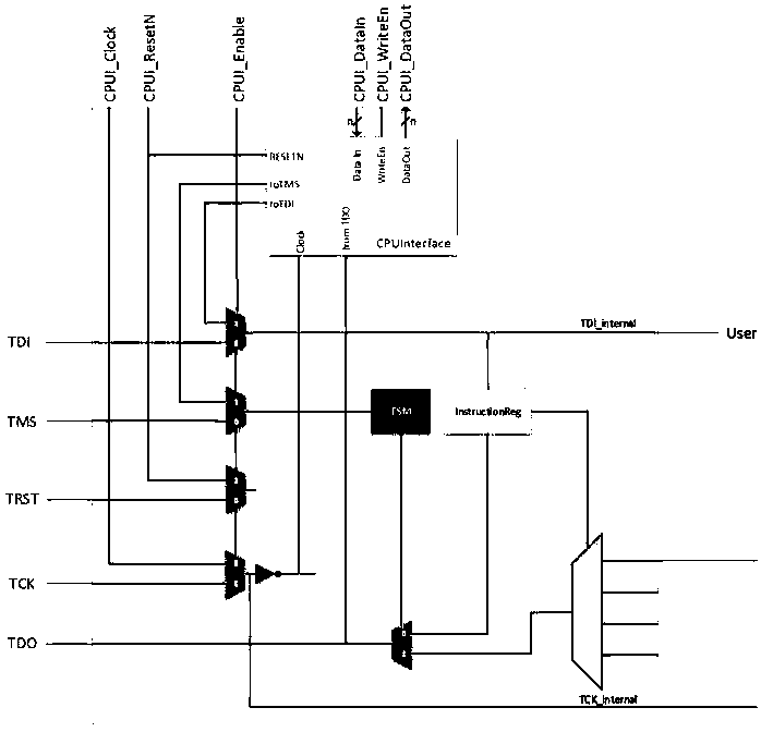
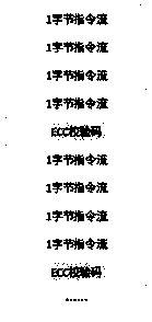
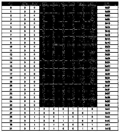
[0050] This embodiment provides an on-chip memory test circuit, such as figure 1 As shown, the on-chip memory test circuit includes an embedded self-test circuit 10, a TAP controller 20, a test instruction conversion circuit 30 and an off-chip Flash40, wherein: the embedded self-test circuit 10 is configured by an EDA tool to the RTL code. The on-chip memory 50 is inserted and formed to generate test vectors; the TAP controller 20 is correspondingly generated when the embedded self-test circuit 10 is formed, and during mass production, the external test device 60 communicates with the TAP controller 20 through the JTAG interface communication, and configure the embedded self-test circuit 10, select to open single or multiple embedded self-test circuits 10 to test the on-chip memory 50; the EDA tool sets the hardware bus width, and uses the first A script converts the test vector into a first test instruction, encapsulates the first test instruction, encodes it and converts it ...

Embodiment 2

[0066] The present embodiment also provides an on-chip memory testing method, the on-chip memory 50 testing method includes: the embedded self-test circuit 10 is formed by inserting the on-chip memory 50 in the RTL code by the EDA tool, and generates test vectors; TAP controller 20 Correspondingly generated when the embedded self-test circuit 10 is formed, during mass production, an external test device communicates with the TAP controller 20 through the JTAG interface, and configures the embedded self-test circuit 10, and selects to open a single or a plurality of embedded self-test circuits 10 to test the on-chip memory 50; the EDA tool sets the hardware bus width, utilizes the first script to convert the test vector into the first test instruction, and converts the second test vector to the first test instruction. A test command is encapsulated, encoded and converted into a binary command stream in bytes, the binary command stream produces a corresponding ECC check code, and...


PUM


Abstract

The invention provides an on-chip memory test circuit and a method thereof. The on-chip memory in the RTL code is inserted by an EDA tool to form an embedded self-test circuit, and a test vector is generated. A TAP control is generated correspondingly when that built-in self-test circuit is for, and the external test equipment communicates with the TAP controller through a JTAG interface in mass production; EDA tool sets hardware bus width, converts test vector into first test instruction by first script, encapsulates first test instruction, encodes and converts into binary instruction streamin bytes, binary instruction stream generates corresponding ECC check code, and stores binary instruction stream into off-chip Flash; The test instruction conversion circuit retrieves the binary instruction stream from the off-chip Flash, parses the binary instruction stream, and transfers the binary instruction stream to the TAP controller through the CPU interface. After receiving the binary instruction stream, the TAP controller configures the embedded self-test circuit to turn on the test function.

Description

technical field [0001] The invention relates to the technical field of chip testing, in particular to an on-chip memory testing circuit and method. Background technique [0002] There are often a large amount of memory inside the chip, and these memories need to be mass-produced and tested before they can be sold to customers. At the same time, customers will also face the possibility of memory aging and failure due to long service life during use. Therefore, during the life cycle of the chip, it is also necessary to test the memory to detect chip failures in time to ensure the normal operation of the chip. [0003] The previous MBIST (memory self-test) circuit usually has two solutions: one is to artificially design a test engine and cover all the memories in the chip. The advantage of this solution is that it can be started at any time (mass production test phase and normal use phase) The test engine tests the internal memory of the chip; the disadvantage is that it is l...

Claims


Application Information

Patent Timeline
Patent Type & Authority Applications(China)
IPC IPC(8): G11C29/10G11C29/42
CPCG11C29/10G11C29/42
Inventor 陈朝杰袁志坚
Owner OMNIVISION TECH (SHANGHAI) CO LTD
Why Eureka
Try Eureka