Formation method for semiconductor devices

A semiconductor and device technology, applied in the field of semiconductor device formation, can solve problems such as inability to form patterns accurately, and achieve the effects of not easy etching loss, improved mechanical properties, and guaranteed accuracy

Active Publication Date: 2019-01-01
SEMICON MFG INT TIANJIN +1
View PDF4 Cites 15 Cited by
  • Summary
  • Abstract
  • Description
  • Claims
  • Application Information

AI Technical Summary

Problems solved by technology

[0005] Embodiments of the present invention provide a method for forming a semiconductor device. Materials with relatively high mechanical properties such as hardness and strength are selected to form a mask layer to improve the ability of the mask layer to resist etching and ensure the size and pattern structure of the mask layer. Accurate, so as to solve the problem that the subsequent pattern cannot be accurately formed

Method used


Image

  • Formation method for semiconductor devices
  • Formation method for semiconductor devices
  • Formation method for semiconductor devices

Examples


Embodiment Construction

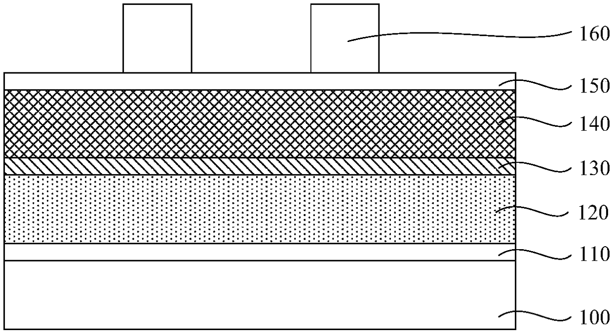
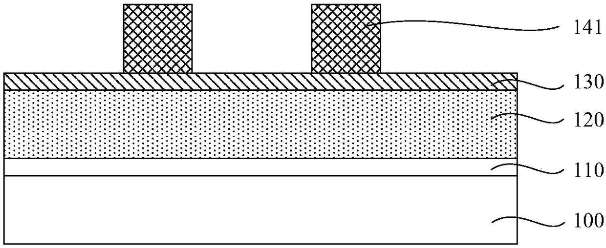
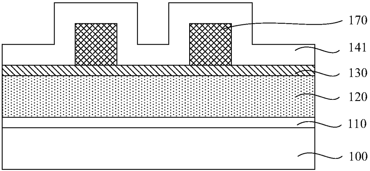
[0035] As mentioned above, the mask layer material used in the existing ASQP process has relatively large loss during the etching process, and the size, structure, and shape of the mask layer have changed greatly, and subsequent patterns cannot be accurately formed.

[0036] Research has found that the reasons for the above problems are: the mechanical properties of the mask layer material used are relatively low in hardness and strength, the material to be etched has relatively small etching options relative to the mask layer, and the mask layer has a relatively low resistance to etching. Weak, easy to be worn out during further etching.

[0037] In order to solve this problem, the present invention provides a mechanical property such as strength and hardness relative to TiO x Higher material ZrO x As a mask layer material. Under the same etching process conditions, the rate at which the mask layer is etched is much lower than the rate at which the material to be etched is etched....


PUM


Abstract

The invention discloses a formation method for semiconductor devices. The formation method includes providing a substrate, and successively forming a first mask material layer, a sacrificial layer anddiscrete photoresist layers on the substrate; taking the discrete photoresist layers as masks to etch the sacrificial layer so that discrete sacrificial layers can be formed; forming first side wallscovering the side wall surfaces of the discrete sacrificial layers; forming second side walls covering the side wall surfaces of the first side walls after removing the discrete sacrificial layers; removing the first side walls through etching, taking the second side walls as the masks to etch the first mask material layer to form first mask layers; forming a second mask material layer covering the surfaces of the first mask layers; and removing part of the second mask material layer until the first mask layers are exposed, and removing the first mask layers through etching to form second mask layers. According to the method, the mechanical properties of the semiconductor device mask layers can be improved, and the accuracy of patterns can be enhanced during transferring.

Description

Technical field [0001] The present invention relates to the field of semiconductor manufacturing, and in particular to a method for forming semiconductor devices. Background technique [0002] In the semiconductor manufacturing process, a photolithography process is usually used to transfer the pattern on the mask to the substrate. With the continuous reduction of the size of semiconductor devices, the critical dimensions of lithography have gradually approached or even exceeded the physical limits of lithography, thus posing more severe challenges to the lithography technology. The Anti-Spacer Quadruple Pattern (ASQP) technology is an important patterning process, which is widely used in the semiconductor back-end manufacturing process (Back-end Of Line, BEOL). ASQP can realize the automatic alignment of the photocopying process, can reduce the size of components, trenches, gates and other structures in the circuit, and can also reduce the size of the target pattern, thereby re...

Claims


Application Information

Patent Timeline
Patent Type & Authority Applications(China)
IPC IPC(8): H01L21/033
CPCH01L21/0332H01L21/0335H01L21/0338
Inventor 张海洋陈卓凡
Owner SEMICON MFG INT TIANJIN
Why Eureka
Try Eureka