Shield grid DMOS device

A shielding gate and device technology, applied in semiconductor devices, electrical components, circuits, etc., can solve the problems of device reliability reduction, switching loss increase, gate-source capacitance increase, etc., to improve switching speed and withstand voltage level, Effect of reducing switching loss and improving contradictory relationship

Active Publication Date: 2019-01-01
UNIV OF ELECTRONICS SCI & TECH OF CHINA
View PDF3 Cites 14 Cited by
  • Summary
  • Abstract
  • Description
  • Claims
  • Application Information

AI Technical Summary

Problems solved by technology

However, the reduction of the gate-to-drain capacitance will make the device more prone to failure when it encounters a large turn-on or turn-off drain-source spike voltage, reducing the reliability of the device
In addition, due to the existence of the polysilicon shield gate under the SGT, the coverage area of ​​the gate and the source is increased, resulting in a large gate-source capacitance of the structure.
Moreover, the reduction of the on-resistance of the conventional SGT depends on the larger cell density. With the reduction of the cell size, the gate-source capacitance of the device will continue to increase, and the device needs a larger gate drive signal to be turned on normally, resulting in Reduced switching speed, increased switching loss, etc.
Therefore, the reduction of on-resistance will increase the gate-source capacitance, and the reduction of gate-drain capacitance will also reduce the reliability of the device. Therefore, it is necessary to reasonably adjust the ratio of gate-source capacitance to gate-drain capacitance to improve conduction. The contradictory relationship between resistance and switching loss

Method used


Image

  • Shield grid DMOS device
  • Shield grid DMOS device
  • Shield grid DMOS device

Examples


Embodiment 1

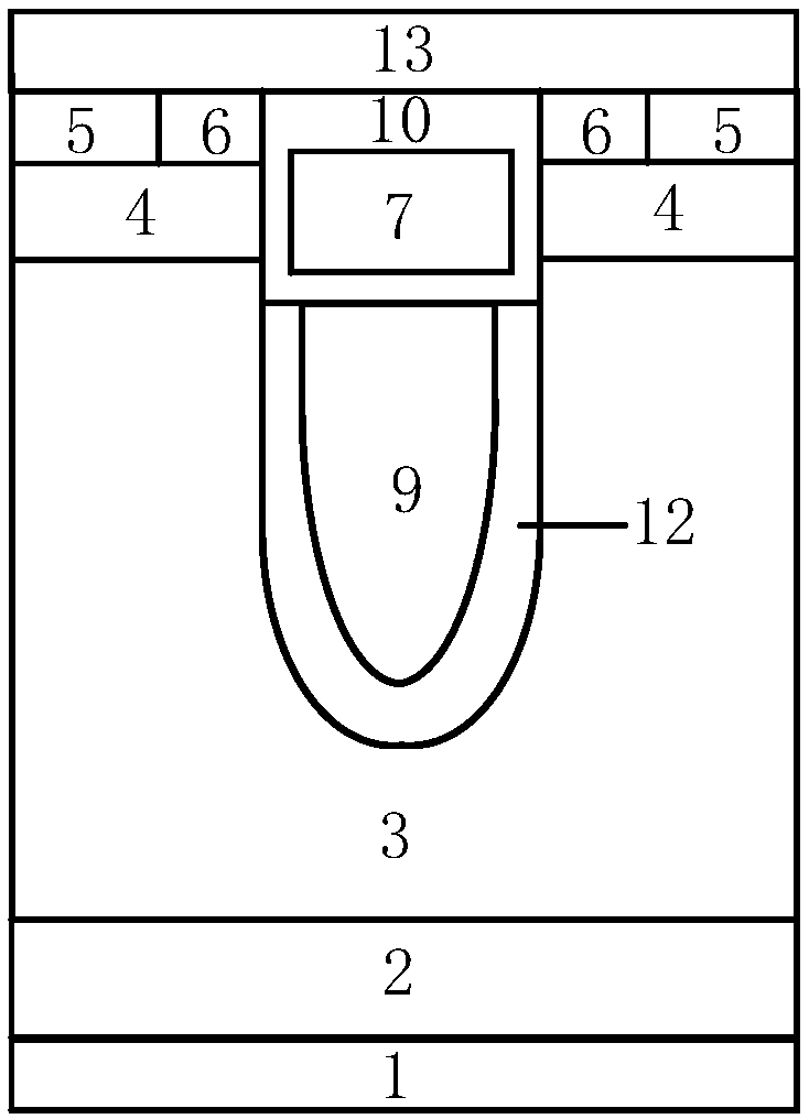
[0022] This embodiment provides a figure 2 The shielded gate DMOS device shown includes a metallized drain 1, a first conductivity type semiconductor heavily doped substrate 2, a first conductivity type semiconductor drift region 3, and a metallization source 13 that are sequentially stacked from bottom to top; The upper layer of the first conductivity type semiconductor drift region 3 has a groove gate structure and a second conductivity type semiconductor body region 4, and the second conductivity type semiconductor body region 4 is located on both sides of the groove gate structure and is in contact with the groove gate structure; The upper layer of the second conductivity type semiconductor body region 4 has a second conductivity type semiconductor heavily doped contact region 5 and a first conductivity type semiconductor heavily doped source region 6, and the first conductivity type semiconductor heavily doped source region 6 is connected to the groove Gate structure con...

Embodiment 2

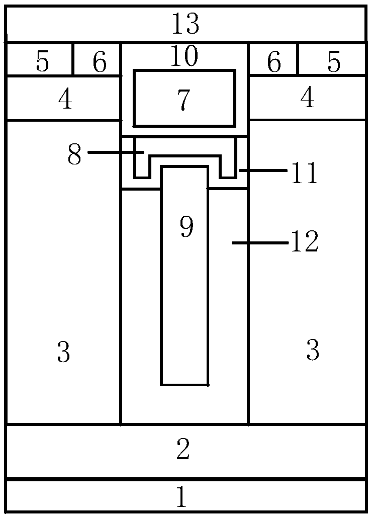
[0027] The embodiment of the present invention is different from the embodiment 1 in that: the shielding gate electrode 9 and the third dielectric layer 12 extend to the bottom of the first conductivity type semiconductor drift region 3, so that the shielding gate electrode 9 is located inside the third dielectric layer 12, The lower surface of the third dielectric layer 12 is in contact with the heavily doped substrate 2 of the first conductivity type semiconductor, such as image 3 shown. This embodiment can achieve a higher doping concentration in the drift region, further reducing the on-resistance of the device.

Embodiment 3

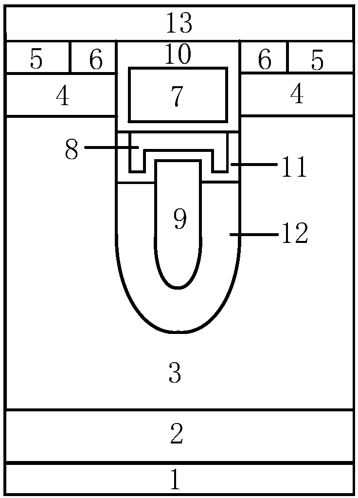
[0029] The difference between the embodiment of the present invention and the embodiment 1 is that the "inverted U-shaped" floating gate electrode 8 is replaced by a rectangular floating gate electrode 8, and the rest of the structure is the same as that of the embodiment 1, as shown in Figure 4 shown. Compared with Embodiment 1, the lateral width of the shielding gate electrode 9 in this embodiment is larger, so the manufacturing process requires less technical level, and the manufacturing process of the rectangular floating gate electrode is simple, which reduces the difficulty of the process. Moreover, the structure can properly reduce the overlapping area between the floating gate electrode and the shielding gate electrode, so as to reduce the total series capacitance value, further reduce the gate-source capacitance, and reduce switching loss.


PUM


Abstract

The present invention provides a shield grid DMOS device, belonging to the technical field of power semiconductors. An extra floating grid electrode is arranged between a control grid electrode and ashield grid electrode, dielectric layers are configured to mutually isolate the electrodes, the floating grid electrode with an adjustable position is introduced, the grid source capacitance of the device is reduced, the specific value of the grid source capacitance and the grid-drain capacitance is adjustable, and the combination of the floating grid electrode and the earthed shield grid electrode allows an electric field in a first conductive type semiconductor drift region to be more uniformly distributed. The shield grid DMOS device reduces the switching loss of the device, improves the device switching speed and voltage withstand level and improves the contradictory relation of the conduction resistance and the switching loss.

Description

technical field [0001] The invention belongs to the technical field of power semiconductors, and in particular relates to a shielded gate DMOS device. Background technique [0002] Power semiconductor devices are semiconductor devices for power processing, which combine microelectronics technology and power electronics technology to form the basis and core of power electronics technology. Power MOSFET plays an important role in the field of power conversion due to its advantages such as fast switching speed, high input impedance, low loss, simple driving, and good frequency characteristics. Its development process is to continuously improve withstand voltage and reduce loss on the basis of maintaining its own advantages. the process of. The traditional VDMOS device is a planar structure using a double-diffusion process. It is the first power MOSFET successfully commercially applied and has played a key role in promoting the development of power MOSFETs. However, the existen...

Claims


Application Information

Patent Timeline
Patent Type & Authority Applications(China)
IPC IPC(8): H01L29/423H01L29/78
CPCH01L29/4236H01L29/7813H01L29/41H01L29/407H01L29/404
Inventor 高巍何文静任敏蔡少峰李泽宏张金平张波
Owner UNIV OF ELECTRONICS SCI & TECH OF CHINA
Why Eureka
Try Eureka