Superjunction device and method of making the same

A super-junction device and charge technology, which is applied in the field of semiconductor integrated circuit manufacturing, can solve the problems affecting the device's ability to resist avalanche breakdown, affect the reliability of the device, and weaken the ability, so as to improve the ability to resist avalanche breakdown and improve the collection ability. Effect

Active Publication Date: 2021-08-31
SHENZHEN SANRISE TECH CO LTD
View PDF17 Cites 0 Cited by
  • Summary
  • Abstract
  • Description
  • Claims
  • Application Information

AI Technical Summary

Problems solved by technology

Usually, the contact hole at the top of the p-type ring will be formed by extending the contact hole at the top of the source region in the charge flow region to the transition region, so this limits the size of the contact hole at the top of the p-type ring. Such a limitation makes The ability of the device to collect electron-hole pairs through the contact hole in the transition region is weakened, which affects the anti-avalanche breakdown capability of the device. At the same time, it also limits the thickness of the interlayer film in the contact hole area of ​​the P-type ring in the transition region. The contact hole in the area should not be too thick to affect the filling ability of subsequent metal deposition in the contact hole, otherwise pinholes may appear in the metal filling due to the high aspect ratio, thus affecting the reliability of the device

Method used


Image

  • Superjunction device and method of making the same
  • Superjunction device and method of making the same
  • Superjunction device and method of making the same

Examples


Embodiment Construction

[0069] The super junction device of the first embodiment of the present invention:

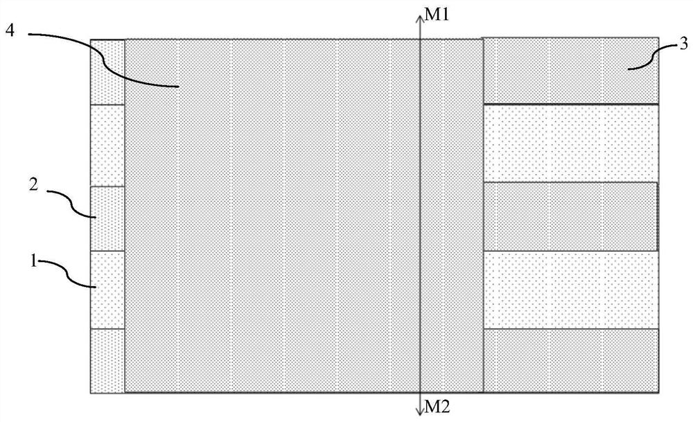
[0070] Such as Image 6 Shown is a top view of the formation area of ​​the source 7a and gate 7b formed by the front metal layer of the superjunction device in the first embodiment of the present invention; in order to more clearly understand the structure of the device in the first embodiment of the present invention, here also combined with Figure 1 to Figure 5 as well as Figure 7 to Figure 10 For explanation, the details are as follows:

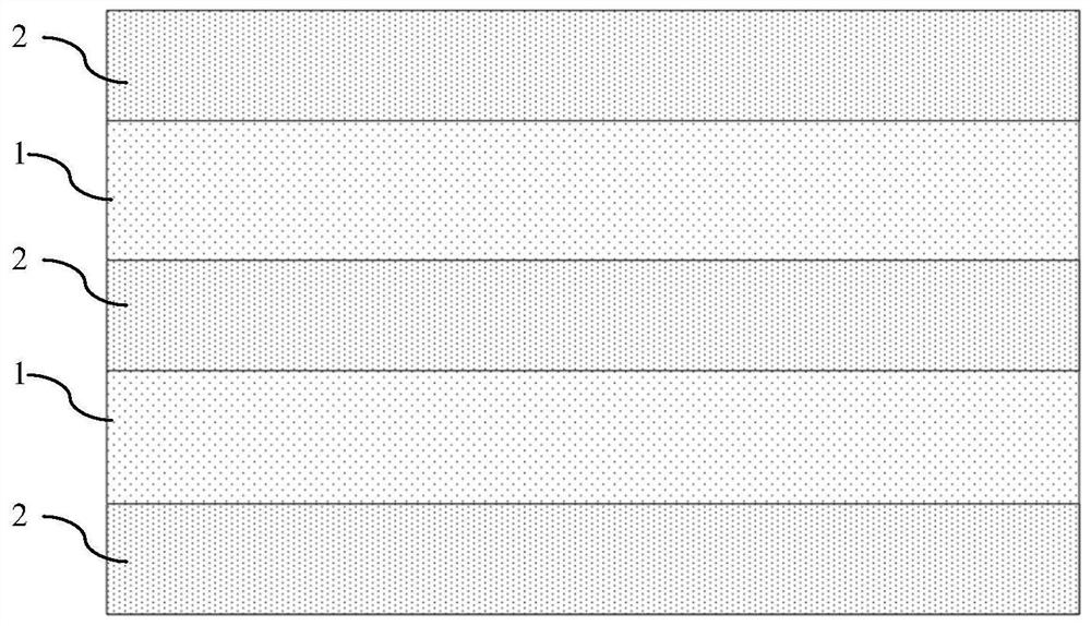
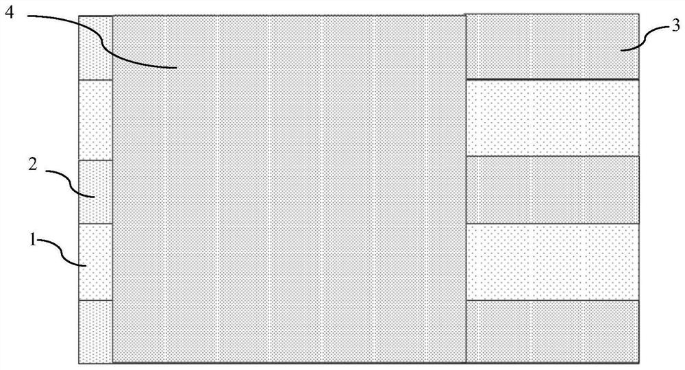
[0071] The super-junction device of the first embodiment of the present invention is described by taking a super-junction MOSFET as an example. The middle region of the super-junction device of the first embodiment of the present invention is the charge flow region, the terminal region surrounds the outer periphery of the charge flow region, and the transition region is located at Between the charge flow region and the termination region; the superjun...


PUM

PropertyMeasurementUnit
thicknessaaaaaaaaaa
thicknessaaaaaaaaaa
thicknessaaaaaaaaaa

Abstract

The invention discloses a superjunction device, which is provided with a protective epoxy film surrounding the charge flow region, so that the JFET region and the source region can be fully injected, and the lateral dimension of the second contact hole in the transition region is larger than The minimum lateral size of the first contact hole in the charge flow region, and ensure that the second contact hole has a smaller aspect ratio under the condition of passing through one more layer of protective epoxy film than the first contact hole, so that both The area of ​​the second contact hole is increased to increase the carrier collection capability of the transition region, and the aspect ratio of the second contact hole can be reduced so that the deeper second contact hole can be filled with pinhole-free metal. The invention also discloses a manufacturing method of the super junction device. The invention can improve the anti-avalanche breakdown capability of the device, and at the same time prevent metal-filled pinholes from appearing in the contact holes in the transition area, improve the reliability of the device, reduce photoetching levels, and reduce process costs.

Description

technical field [0001] The invention relates to a method for manufacturing a semiconductor integrated circuit, in particular to a method for manufacturing a superjunction device. Background technique [0002] In existing super junction devices, in the current flow area, there are alternately arranged P-type columns and N-type columns. Taking strip-shaped P-N columns that are alternately arranged P-type columns and N-type columns as an example, each N There is a polysilicon gate above the pillar, which can partially cover the surrounding P pillars or not. There is a P-type well (PWell) above each P-pillar, and there is an N+ source region in the P-type well. There is a contact hole, the source metal is connected to the source region through the contact hole, the source metal is connected to the P region, that is, the P-type well, through a high-concentration P+ contact region, and the source metal is the front metal layer that forms the source. [0003] There is a transition...

Claims


Application Information

Patent Timeline
Patent Type & Authority Patents(China)
IPC IPC(8): H01L29/06H01L29/78H01L21/336
CPCH01L29/0634H01L29/66712H01L29/7803
Inventor 肖胜安曾大杰李东升郑怡
Owner SHENZHEN SANRISE TECH CO LTD
Why Eureka
Try Eureka