TiN Thin Film Etching Method

A thin film, dry etching technology, applied in decorative arts, gaseous chemical plating, microstructure technology, etc., can solve problems such as hindering the etching of TiN thin films

Inactive Publication Date: 2019-01-08
SHANGHAI HUAHONG GRACE SEMICON MFG CORP
View PDF4 Cites 1 Cited by
  • Summary
  • Abstract
  • Description
  • Claims
  • Application Information

AI Technical Summary

Problems solved by technology

[0002] As a relatively high-resistance film, TiN film is often used as an electrode in MEMS (micro-electromechanical system) devices. Due to the special structure of the TiN film itself, there will be some N (nitrogen) in TiN in the process of being bombarded by oxygen-containing ions. Atoms are replaced to form a special film with oxygen covering the surface of TiN, which will seriously hinder the etching of TiN film during the subsequent etching process

Method used


Image

  • TiN Thin Film Etching Method

Examples


Embodiment Construction

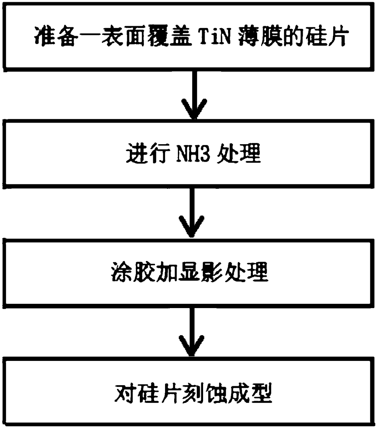
[0013] combine figure 1 As shown, the TiN thin film etching method is in the following examples, and the specific implementation process is as follows:

[0014] Step 1. Prepare a silicon substrate covered with a TiN thin film, that is, a silicon wafer covered with a TiN thin film. The thickness of the TiN thin film is 10-30 nm. The film-forming method of the TiN thin film is not limited to one of film-forming methods such as physical deposition (PVD) and chemical vapor deposition (CVD) or a mixed process method.

[0015] Step 2, performing NH3 treatment on the silicon wafer covered with TiN thin film. The equipment for NH3 treatment of silicon wafers covered with TiN film is CVD equipment process chamber or PVD equipment process chamber, the treatment process temperature is 250-400°C, the vacuum pressure is 3-10torr, the flow rate of NH3 is 30-100sccm, and the flow rate of N2 is 3 ~10k sccm, processing time is 10~30s.

[0016] Step 3, coating and developing the silicon waf...


PUM

PropertyMeasurementUnit
thicknessaaaaaaaaaa

Abstract

The invention discloses a TiN thin film etching method, comprising the following steps: step 1, carrying out NH3 treatment on a silicon wafer covered with the TiN thin film; 2, coating the NH3-treatedsilicon wafer with glue and carrying out development treatment on the silicon wafer; 3, etch and molding that silicon wafer. The invention can effectively etch the TiN film without affecting the characteristics of the lower film.

Description

technical field [0001] The invention relates to the field of semiconductor integrated circuits, in particular to a TiN (titanium nitride) film etching method. Background technique [0002] As a relatively high-resistance film, TiN film is often used as an electrode in MEMS (micro-electromechanical system) devices. Due to the special structure of the TiN film itself, there will be some N (nitrogen) in TiN in the process of being bombarded by oxygen-containing ions. The atoms are replaced to form a special film with oxygen covering the surface of TiN, which will seriously hinder the etching of the TiN film during the subsequent etching process. Contents of the invention [0003] The technical problem to be solved by the present invention is to provide a TiN thin film etching method, which can effectively etch away the TiN thin film without affecting the properties of the underlying thin film. [0004] In order to solve the above-mentioned technical problems, the TiN film et...

Claims


Application Information

Patent Timeline
Patent Type & Authority Applications(China)
IPC IPC(8): H01L21/311B81C1/00
CPCB81C1/00523H01L21/31111H01L21/31116H01L21/31122H01L21/31144
Inventor 刘善善朱黎敏朱兴旺
Owner SHANGHAI HUAHONG GRACE SEMICON MFG CORP
Why Eureka
Try Eureka