Organic electroluminescent device and preparation method thereof

An electroluminescent device and a luminescent technology, which can be used in organic light-emitting devices, organic semiconductor devices, electric solid-state devices, etc., and can solve problems such as lifespan decline

Active Publication Date: 2019-01-15
KUNSHAN GO VISIONOX OPTO ELECTRONICS CO LTD
View PDF13 Cites 1 Cited by
  • Summary
  • Abstract
  • Description
  • Claims
  • Application Information

AI Technical Summary

Problems solved by technology

[0004] Based on this, it is necessary to provide an organic electroluminescent device and its preparation method that can improve the lifespan in view of the serious problem of life-span degradation of traditional organic electroluminescent devices

Method used


Image

  • Organic electroluminescent device and preparation method thereof
  • Organic electroluminescent device and preparation method thereof
  • Organic electroluminescent device and preparation method thereof

Examples


Embodiment approach 1

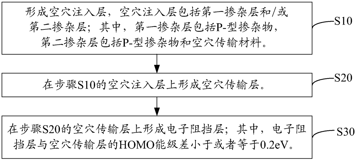
[0043] The organic electroluminescent device of Embodiment 1 includes an anode and a hole injection layer, a hole transport layer, an electron blocking layer, an organic light emitting layer, an electron transport layer and a cathode formed sequentially on the anode.

[0044] Wherein, the hole injection layer includes a first doped layer. The first doped layer includes P-type dopants. The P-type dopant can increase the amount of hole injection, thereby increasing the lifetime of mass-produced devices.

[0045] On the basis of the foregoing embodiments, the hole injection layer is composed of the first doped layer. The first doped layer is composed of P-type dopants. At this time, only the P-type dopant is contained in the first doped layer, which is more conducive to increasing the injection amount of holes, thereby improving the lifespan of mass-produced devices. It should be noted that, the P-type dopant in this embodiment may contain a small amount of impurities within t...

Embodiment approach 2

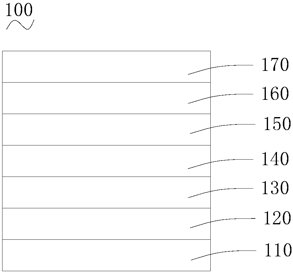
[0073] The difference between the organic electroluminescent device of the second embodiment and the organic electroluminescent device of the first embodiment is that the hole injection layer includes a second doped layer. The second doped layer includes a P-type dopant and a hole transport material. By adjusting the doping concentration of the P-type dopant, the injection amount of holes can be controlled, thereby adjusting the balance of electrons and holes, thereby improving the lifespan of mass-produced devices.

[0074] On the basis of the foregoing embodiments, the hole injection layer is composed of the second doped layer. The second doped layer consists of P-type dopants and hole transport material. At this time, the second doped layer only contains P-type dopants and hole transport materials, which is more conducive to controlling the injection of holes, thereby adjusting the balance of electrons and holes, thereby improving the life of mass-produced devices . It s...

Embodiment approach 3

[0091] The difference between the organic electroluminescent device of Embodiment 3 and the organic electroluminescent devices of Embodiment 1 and Embodiment 2 is that the hole injection layer includes a first doped layer and a second doped layer formed on the first doped layer. a doped layer, the second doped layer is close to the hole transport layer.

[0092] On the basis of the foregoing embodiments, the thickness of the first doped layer is 1 nm˜10 nm, and the thickness of the second doped layer is 10 nm˜20 nm.

[0093] The organic electroluminescent device of Embodiment 3 can adjust the injection amount of holes, and at the same time improve the efficiency and lifetime of the device. The difference between the organic electroluminescent device of the fourth embodiment and the organic electroluminescent device of the third embodiment is that the hole injection layer includes a second doped layer and a first doped layer formed on the second doped layer, and the second dope...


PUM

PropertyMeasurementUnit
Thicknessaaaaaaaaaa
Thicknessaaaaaaaaaa
Thicknessaaaaaaaaaa

Abstract

The invention relates to an organic electroluminescent device and a preparation method thereof. Includes a hole injection layer including a first doped layer and / or a second doped layer; Wherein the first doped layer comprises P-Type dopant; The second doping layer comprises P-Type dopants and hole transport materials; A hole transport layer formed on the hole injection layer; And an electron blocking layer formed on the hole transport layer; Where the HOMO energy level difference between the electron blocking layer and the hole transport layer is less than or equal to 0.2 eV. In the first doped layerP-Type dopant can increase the hole injection quantity, thus prolonging the lifetime of mass-produced devices; In the second doped layer, by adjusting the The doping concentration of the dopant can control the amount of holes injected, which can adjust the balance of electrons and holes, and then prolong the lifetime of mass-produced devices. At the same time, the HOMO energy level difference between the electron barrier layer and the hole transport layer is less than or equal to 0.2 eV, which can reduce the power consumption of the organic electroluminescent devices and thus prolong the lifetime of the mass-produced devices.

Description

technical field [0001] The invention relates to the technical field of light emitting devices, in particular to an organic electroluminescent device and a preparation method thereof. Background technique [0002] Organic electroluminescence refers to the phenomenon that organic light-emitting materials emit light under the excitation of electric current or electric field. Organic electroluminescent devices (OLED, Organic Light-Emitting Diode) have active luminescence, high luminous efficiency, fast response time (on the order of 1μs), low operating voltage (3v~10v), wide viewing angle (>175°above), panel Thin thickness (<1mm), low power consumption, wide operating temperature range (-40℃~﹢85℃), and flexible display can be realized, so it has attracted widespread attention. [0003] After the traditional organic electroluminescent devices are introduced into mass production, the lifespan decreases seriously. The lifespan of LT97 is often lower than 180 hours, which is ...

Claims


Application Information

Patent Timeline
IPC IPC(8): H01L51/50H01L51/56
CPCH10K50/155H10K50/18H10K50/00H10K2102/301H10K71/00C09K11/06H10K50/11H10K2101/40H10K50/15H10K50/17H10K50/80H10K85/631H10K85/657H10K85/6572H10K50/157H10K85/633H10K85/654H10K85/615H10K2101/30
Inventor 李维维刘胜芳闵超徐磊高孝裕黄秀颀
Owner KUNSHAN GO VISIONOX OPTO ELECTRONICS CO LTD
Why Eureka
Try Eureka