
Semiconductor device and manufacturing method thereof

A manufacturing method and semiconductor technology, applied in semiconductor devices, electrical components, circuits, etc., can solve the problems of large leakage current and low breakdown electric field strength, and achieve the effects of reducing parasitic capacitance, suppressing leakage current, and improving mechanical strength

Active Publication Date: 2021-11-23
GUANGDONG INST OF SEMICON IND TECH
View PDF4 Cites 0 Cited by
  • Summary
  • Abstract
  • Description
  • Claims
  • Application Information

AI Technical Summary

Problems solved by technology

Moreover, the silicon substrate has a certain conductivity, and the breakdown electric field strength is low, which leads to a large leakage current between the silicon substrate and the drain of the HEMT or the anode of the Schottky diode.

Method used


Image

  • Semiconductor device and manufacturing method thereof
  • Semiconductor device and manufacturing method thereof
  • Semiconductor device and manufacturing method thereof

Examples


Embodiment Construction

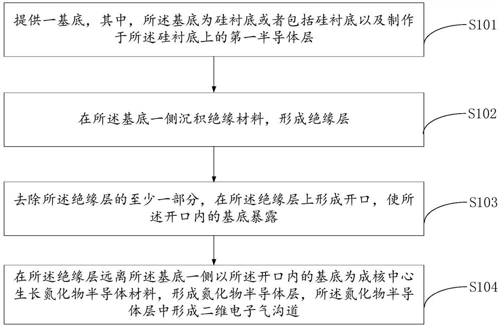
[0087] The following will clearly and completely describe the technical solutions in the embodiments of the present invention with reference to the accompanying drawings in the embodiments of the present invention. Obviously, the described embodiments are only some, not all, embodiments of the present invention. The components of the embodiments of the invention generally described and illustrated in the figures herein may be arranged and designed in a variety of different configurations. Accordingly, the following detailed description of the embodiments of the invention provided in the accompanying drawings is not intended to limit the scope of the claimed invention, but merely represents selected embodiments of the invention. Based on the embodiments of the present invention, all other embodiments obtained by those skilled in the art without making creative efforts belong to the protection scope of the present invention.

[0088] It should be noted that like numerals and let...


PUM


Abstract

The invention provides a semiconductor device and a manufacturing method thereof, which relate to the technical field of semiconductors. In the semiconductor device manufactured by the manufacturing method in the embodiment of the present application, there is an insulating layer between the substrate and the subsequent epitaxial structure, and the insulating layer can effectively suppress the doping of the silicon substrate during the nitride epitaxial growth process, thereby Reduce the free carriers introduced into the silicon substrate, greatly reduce the electrical signal response of the silicon substrate on the epitaxial structure, and greatly reduce the parasitic capacitance of the device. At the same time, the insulating layer can effectively suppress the leakage current through the silicon substrate in the device. In addition, the nitride semiconductor layer in the present application is obtained by growing the substrate in the opening on the insulating layer as a nucleation center, so that the nitride semiconductor layer has better crystal quality.

Description

technical field [0001] The present invention relates to the technical field of semiconductors, in particular to a semiconductor device and a manufacturing method thereof. Background technique [0002] Group III nitride semiconductor is an important semiconductor material, mainly including AlN, GaN, InN and compounds of these materials such as AlGaN, InGaN, AlInGaN and so on. III / V compound semiconductors have broad applications in light emitting devices, power electronics, radio frequency devices and other fields. [0003] An important device type of III-nitride semiconductors are III-nitride high electron mobility transistors (HEMTs) and Schottky diodes, which have great prospects in the field of power semiconductors. Since gallium nitride bulk materials are extremely expensive, an economical approach is to epitaxially grow nitride semiconductor materials on heterogeneous substrates and fabricate device structures such as electrodes. Common substrate materials are alumina...

Claims


Application Information

Patent Timeline
Patent Type & Authority Patents(China)
IPC IPC(8): H01L29/06H01L29/778H01L29/872
CPCH01L29/0603H01L29/0684H01L29/778H01L29/872
Inventor 黎子兰刘小平张树昕
Owner GUANGDONG INST OF SEMICON IND TECH
Learn More