

Contact-passivation crystalline silicon solar cell structure and preparation method
A technology of solar cells and crystalline silicon, applied in the field of solar cells, can solve the problems of affecting the collection of carriers and requiring high film thickness, and achieve the effects of good light trapping, improving comprehensive performance and improving carrier transport capability.
- Summary
- Abstract
- Description
- Claims
- Application Information
AI Technical Summary
Problems solved by technology
Method used
Image

Examples
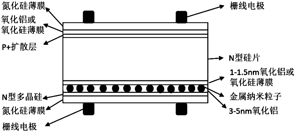
Embodiment 1
[0040] 1. Double-sided texturing of N-type silicon wafers, followed by RCA cleaning
[0041] 2. The silicon wafer enters the diffusion tube for B diffusion, and a pn junction is formed on the light-receiving surface
[0042] 3. Use single-sided etching equipment to protect the surface B of the silicon wafer with a water film, and use alkali or acid to remove the expanded junction on the back to form a polished surface. Finally, the borosilicate glass BSG on the light-receiving surface is removed by HF
[0043] 4. Prepare an aluminum oxide film on the back, using ALD, with a thickness of about 1.5nm, (you can also use hot nitric acid oxidation, or ultraviolet ozone treatment to form an ultra-thin silicon oxide film)
[0044] 5. A 5nm Ag film is prepared by thermal evaporation on the back of the silicon wafer, and then annealed at 500°C to form metal nanoparticles. The annealing process can also enhance the passivation effect of the passivation film;
[0045] 6. Prepare aluminu...
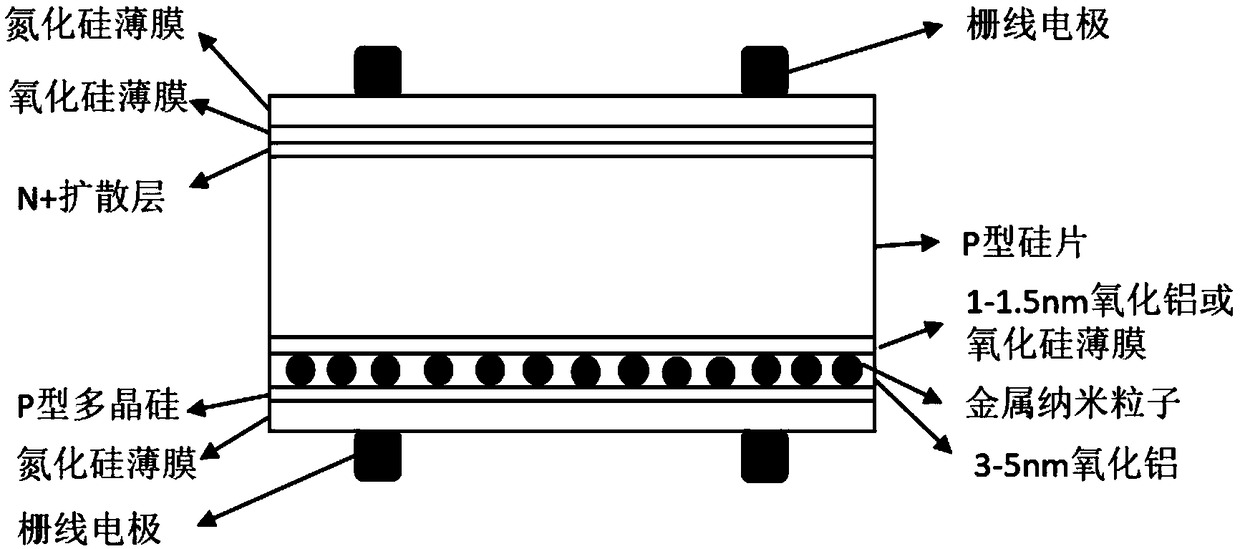
Embodiment 2
[0051] 1. Double-sided texturing of P-type silicon wafers, followed by RCA cleaning
[0052] 2. The silicon wafer enters the diffusion tube for P diffusion, and a pn junction is formed on the light-receiving surface
[0053] 3. Use single-side etching equipment to protect the front P of the silicon wafer with a water film, and use alkali or acid to remove the wound junction on the back to form a polished surface, and finally remove the front phosphosilicate glass PSG by HF
[0054]4. Prepare an aluminum oxide film on the back, using ALD, with a thickness of about 1.5nm, (you can also use hot nitric acid oxidation, or ultraviolet ozone treatment to form an ultra-thin silicon oxide film)
[0055] 5. A 5nm Al film is prepared by thermal evaporation on the back of the silicon wafer, and then annealed at 500°C to form metal nanoparticles. The annealing process can also enhance the passivation effect of the passivation film.
[0056] 6. Prepare an aluminum oxide thin film on the ba...
PUM
| Property | Measurement | Unit |
|---|---|---|
| thickness | aaaaa | aaaaa |
| thickness | aaaaa | aaaaa |
| thickness | aaaaa | aaaaa |
Abstract
Description
Claims
Application Information