
A carbon film spray tin printed circuit board preparation process

A technology of printed circuit board and preparation process, which is applied in the direction of printed circuit manufacturing, printed circuit, and secondary treatment of printed circuit, etc. It can solve the problem of no copper surface roughness, unfavorable carbon film board curing effect, unfavorable carbon film and copper surface Bonding etc.

Active Publication Date: 2021-06-29
ZHENJIANG HUAYIN PRINTED CIRCUIT BOARD
View PDF9 Cites 0 Cited by
  • Summary
  • Abstract
  • Description
  • Claims
  • Application Information

AI Technical Summary

Problems solved by technology

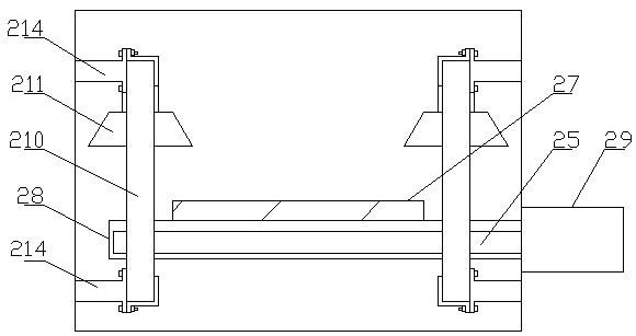
[0004] 1. Before solder mask and carbon film printing, most manufacturers generally use paulownia boards for production without increasing the roughness of the copper surface, which is not conducive to the bonding force between the carbon film and the copper surface during subsequent carbon film printing. And currently there is no special equipment for adjusting and increasing the roughness of the copper surface;
[0005] 2. The current carbon film plate needs to be cured after the tin spraying process, but there is currently no special curing machine for carbon film plate tin spraying. Now the common multi-stage curing machine on the market will easily produce The temperature difference, that is, the temperature at the exit and entrance of the drying tunnel is low, and the temperature at the center of the drying tunnel is high. This temperature difference can often reach more than 20°C, which is not conducive to the final curing effect of the carbon film plate.

Method used


Image

  • A carbon film spray tin printed circuit board preparation process
  • A carbon film spray tin printed circuit board preparation process
  • A carbon film spray tin printed circuit board preparation process

Examples


Embodiment Construction

[0050] In order to make the technical solution of the present invention more clearly, the present invention will be further described below with reference to the drawings, and the techniques of the technical features of the present invention are equivalent replacement and conventional reasoning results in the scope of the invention.

[0051] A carbon film spray printing circuit board preparation process, the steps are as follows:

[0052] (1) Preprocessing: The copper plate matrix is ​​used for mechanical grinding and cleaning the copper plate base before printing and carbon film is printed;

[0053] (2) Preparation Printing Net Edition: 220 ocolina net plate, coated 30UM thickness sealing gel;

[0054] (3) Printing and soldering: printing ink in the printing net; printed on the printing net plate with printing ink is printed on the copper matrix; the copper plate is printed, the solder welding character;

[0055] (4) Curing bake: Add the copper plate base to the seven-temperature...


PUM


Abstract

The preparation process of a carbon film spray tin printed circuit board of the present invention, the steps are as follows: pretreatment: before the solder resist and carbon film printing, the copper plate substrate is mechanically brushed and cleaned by a mechanical brush roughening cleaning machine; preparation Printing screen: use 220-mesh acrylic screen, coated with 30um thickness sealing glue; printing solder mask: print ink on the printing screen; then print the printing screen with printing ink on the copper plate substrate; copper plate substrate printing Finally, solder resist characters; curing and baking: add the copper plate substrate to the circulating hot air curing machine in the seven temperature zones for curing; spray tin: spray tin on the copper plate substrate, and then cool it after spraying tin. The product prepared by this process has a short production cycle, avoids the high pollution of chemical gold, solves the difficulty that the copper surface of the ordinary carbon film plate is easy to oxidize, and improves the overall performance and reliability of the product.

Description

Technical field [0001] The present invention relates to a carbon film spray printing circuit board preparation process. Background technique [0002] At present, the remote control of household appliances, washing machine control panels, etc., all of which are common carbon film, and the copper surface of such carbon film is easily oxidized, which ultimately leads to poor product; and high-end products are generally used by gold plates, and their cost is high. The main raw materials used in the golden gold are cyanide as potassium as a highly toxic substance, store safety hazards, and severely pollute the environment during production, and does not meet the development trend of green production. Carbon plate spraying can solve the problem of oxidation of copper surface of ordinary carbon plates, and avoid high pollution production in the production of gold. However, the traditional carbon film printed circuit board cannot withstand the high temperature impact of spray, which is e...

Claims


Application Information

Patent Timeline
Patent Type & Authority Patents(China)
IPC IPC(8): H05K3/24B08B1/00B08B1/04
CPCB08B1/002B08B1/04H05K3/245
Inventor 李军
Owner ZHENJIANG HUAYIN PRINTED CIRCUIT BOARD
Learn More