Eureka AIR delivers breakthrough ideas for toughest innovation challenges, trusted by R&D personnel around the world.

Semiconductor structure and forming method thereof

A technology of semiconductor and interconnection structure, which is applied in the direction of semiconductor devices, semiconductor/solid-state device manufacturing, semiconductor/solid-state device components, etc. It can solve problems such as large differences in top size and achieve the effect of improving performance

Active Publication Date: 2019-03-05
SEMICON MFG INT (SHANGHAI) CORP +1
View PDF3 Cites 2 Cited by
  • Summary
  • Abstract
  • Description
  • Claims
  • Application Information

AI Technical Summary

Problems solved by technology

[0004] However, the bottom size and top size of the through hole formed by the dual damascene process in the prior art are quite different

Method used


Image

  • Semiconductor structure and forming method thereof
  • Semiconductor structure and forming method thereof
  • Semiconductor structure and forming method thereof

Examples


Embodiment Construction

[0034] As mentioned in the background, the size of the bottom of the through hole is quite different from the size of the top.

[0035] Figure 1 to Figure 2 It is a structural schematic diagram of a method for forming a semiconductor structure.

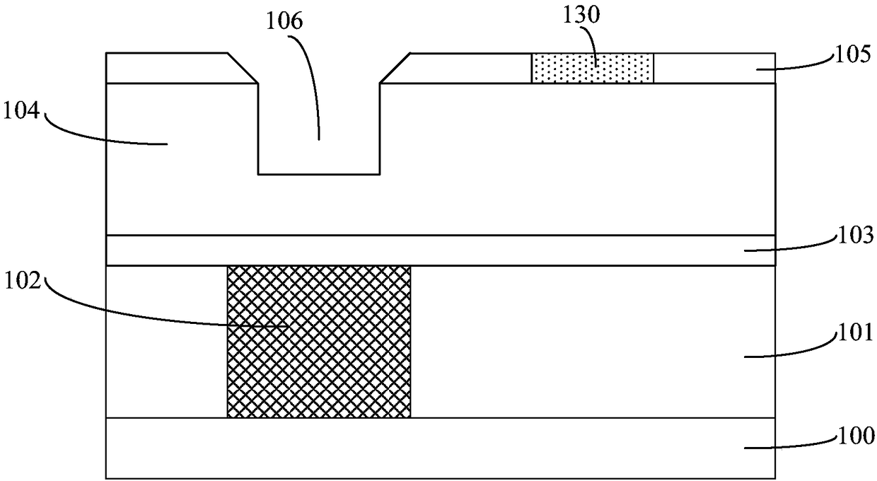
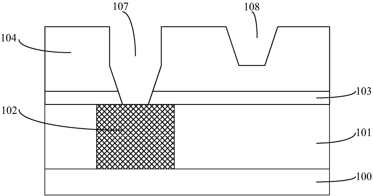
[0036] Please refer to figure 1 , providing a substrate 100, the substrate 100 has a first dielectric layer 101, and the first dielectric layer 101 has a first opening (not marked in the figure); a first interconnection structure is formed in the first opening 102: Form a stop layer 103 and a second dielectric layer 104 on the stop layer 103 on the first dielectric layer 101 and the first interconnection structure 102, the top of the second dielectric layer 104 has a mask layer 105, so There are a first mask opening (not marked in the figure) and a second mask opening (not marked in the figure) in the mask layer 105; a sacrificial layer 130 is formed in the second mask opening; The sacrificial layer 130 and the mask layer 105 are ...


PUM

PropertyMeasurementUnit
Thicknessaaaaaaaaaa
Thicknessaaaaaaaaaa

Abstract

The present invention discloses a semiconductor structure and forming method of the semiconductor structure, the method comprises: providing a substrate, wherein the substrate has a first interconnectstructure; forming a first stop layer on the first interconnect structure; forming a first dielectric layer on the substrate and the first stop layer; using a first etching process to etch the firstdielectric layer on the first interconnect line until the first stop layer is exposed, and forming a first opening inside the first dielectric layer; and using a second etching process to etch the first dielectric layer, forming a groove in the first dielectric layer, etching the first stop layer at bottom of the first opening until the first interconnect structure is exposed, and forming a through hole in the first stop layer and the first dielectric layer, wherein the through hole is in communication with the groove. Components formed by the method have better performance.

Description

technical field [0001] The invention relates to the field of semiconductor manufacturing, in particular to a semiconductor structure and a forming method thereof. Background technique [0002] With the development of semiconductor technology, semiconductor devices have a deep submicron structure, and semiconductor integrated circuits (ICs) contain a huge number of semiconductor elements. In this large-scale integrated circuit, not only single-layer interconnection structures but also multi-layer interconnection structures are protected. The multilayer interconnection structures are stacked on each other, and are isolated by a dielectric layer between the multilayer interconnection structures. In particular, when using a dual-damascene process to form a multilayer interconnection structure, it is necessary to form trenches and via holes for interconnection in the dielectric layer in advance, and then fill the trenches and vias with conductive materials such as copper. throu...

Claims


Application Information

Patent Timeline
IPC IPC(8): H01L21/768H01L23/528
CPCH01L21/76807H01L21/76813H01L23/528
Inventor 周俊卿张海洋
Owner SEMICON MFG INT (SHANGHAI) CORP
Why Eureka
Eureka Blog
Learn More