

Method for rapid imaging of absorption defect distribution on surface of large-diameter optical element
A technology of optical components and defect distribution, applied in the direction of optical testing defects/defects, material thermal development, etc., can solve the problems of extremely long time, lack of technical reality, discount of random characterization effect, etc., to achieve high sensitivity, high Spatial resolution, improving the effect of single detection area
- Summary
- Abstract
- Description
- Claims
- Application Information
AI Technical Summary
Problems solved by technology
Method used
Image

Examples
Embodiment Construction
[0024] Combine below Figure 1-3 Specifically describe a method for rapid imaging of the surface and subsurface absorption defect distribution of a large-aperture optical element proposed by the present invention. However, it should be understood that the accompanying drawings are only provided for better understanding of the present invention, and should not be construed as limiting the present invention. The specific implementation steps are as follows:
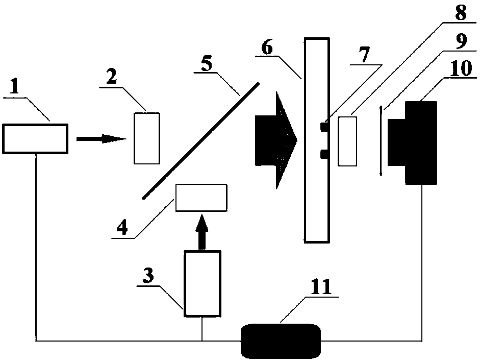
[0025] (1) Build the experimental system. build as figure 1 The shown experimental system of pulse excitation and pulse detection photothermal lens technology based on area array detector includes excitation laser 1 and its collimator beam expansion system 2, detection laser 3 and its collimation beam expansion system 4, beam combiner 5 , 4f system 8, narrow band filter 9, CCD10, and synchronization system 11.
[0026] a. Adjust the excitation laser 1 so that it is incident on the surface of the sample at a certain angl...
PUM
 Abstract
Description
Claims
Application Information