
Mask plate, wafer, crystal grains and plasma etching and splitting method

A technology of plasma and mask, which is applied in the field of ion etching fragments, can solve the problems of increasing crystal grains, increasing grinding time, and reducing wafer efficiency, and achieves the effects of reducing force, reducing risk, and increasing area

Active Publication Date: 2019-03-08
SHANGHAI HUAHONG GRACE SEMICON MFG CORP
View PDF5 Cites 1 Cited by
  • Summary
  • Abstract
  • Description
  • Claims
  • Application Information

AI Technical Summary

Problems solved by technology

[0004] The inventors have found that, in the process before the etching process before grinding, when the wafer is cut by plasma, at the crossing position of the dicing road, the groove depth of the plasma-etched slice is deeper than the groove depth of the non-crossing position, especially at the junction The groove depth of the point is the deepest, especially in the second plasma etching, that is, substrate etching, the depth of the intersection position of the scribe line is deeper than the depth of the non-intersection position, resulting in the subsequent grinding process, the intersection position of the scribe line Grinding through first causes unseparated wafers to shake and reduce wafer efficiency, thereby increasing grinding time and reducing production efficiency. At the same time, it increases the risk of grain fragmentation during grinding. The collision between grains also has the risk of grain fragmentation, which affects the quality of grains

Method used


Image

  • Mask plate, wafer, crystal grains and plasma etching and splitting method
  • Mask plate, wafer, crystal grains and plasma etching and splitting method
  • Mask plate, wafer, crystal grains and plasma etching and splitting method

Examples


Embodiment Construction

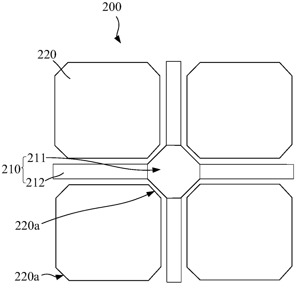
[0042] As described in the background art, in plasma cutting wafers, such as etching before grinding, since the crossing position of the cutting line is the intersection of several cutting lines, the plasma in the non-crossing position converges at the crossing position, As a result, the plasma concentration at the crossing position is much higher than that at the non-crossing position, so that when the substrate is etched, the groove depth at the crossing position is too deep than that at the non-crossing position. During the grinding process, the four corners of most dies on the wafer are the first to wear through. With the continuation of the grinding process, when all the grains are about to be separated, the gap between the grains becomes larger and larger, and there will be mutual extrusion between the grains, so that the grains collide with each other; After the crystal grains are separated, the grains will also collide with each other when taking the chip. The above-me...


PUM

PropertyMeasurementUnit
Depthaaaaaaaaaa

Abstract

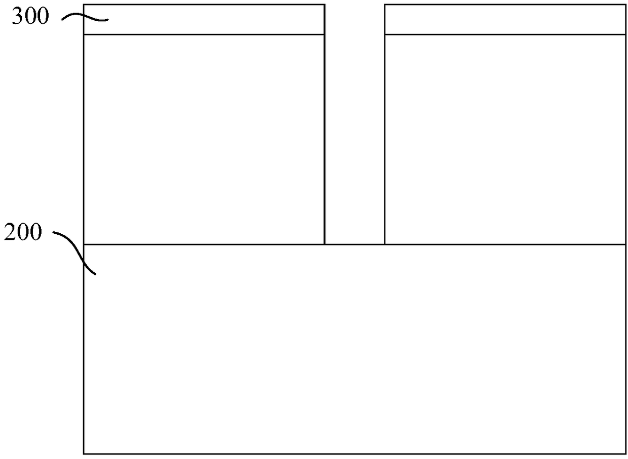
The invention provides a mask plate, a wafer, crystal grains and a plasma etching and splitting method. The mask plate comprises a plurality of crystal grain patterns and a cutting path pattern positioned between the adjacent crystal grain patterns, wherein the cutting path pattern comprises a cross position pattern and a non-cross position pattern, the cross position pattern is positioned among the adjacent four crystal grain patterns and is connected with the adjacent non-cross position pattern, and the crystal grain patterns and the cross position pattern are squares with missing angles. Thereby, the area of the cross positions of cutting paths can be increased, and meanwhile, the acting force of mutual collision among the crystal grains in the crystal grain grinding process and the subsequent packaging process can be reduced, and the risk of crystal grain fragmentation can be further reduced.

Description

technical field [0001] The invention relates to the field of semiconductor integrated circuit manufacturing, in particular to a mask plate, wafer, crystal grain and a method for plasma etching splits. Background technique [0002] An integrated circuit is formed on a wafer, and a semiconductive, conductive or insulating material layer formed on the wafer is usually processed by processes such as doping, deposition, photolithography, and etching to form an integrated circuit. Each wafer is processed to form a large number of individual regions containing integrated circuits, which are also called die. [0003] After the integrated circuit formation process, the wafer is diced to separate the dies from each other for subsequent packaging or packaging for use in larger circuits. Wafer dicing is performed by moving across the wafer surface along pre-formed scribe lines that extend along the spaces between wafers, often referred to as "dicing streets". Plasma dicing is a more c...

Claims


Application Information

Patent Timeline
IPC IPC(8): G03F1/38H01L21/78
CPCG03F1/38H01L21/78
Inventor 高超
Owner SHANGHAI HUAHONG GRACE SEMICON MFG CORP
Learn More