Thin film transistor, its manufacturing method and electronic device
A technology for thin film transistors and manufacturing methods, which are applied in transistors, semiconductor/solid-state device manufacturing, circuits, etc., and can solve problems such as hump effect
- Summary
- Abstract
- Description
- Claims
- Application Information
AI Technical Summary
Problems solved by technology
Method used
Image

Examples
no. 1 example
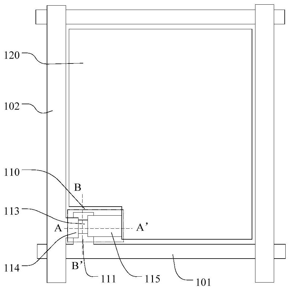
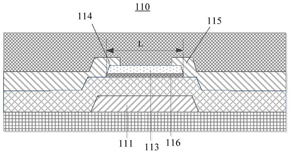
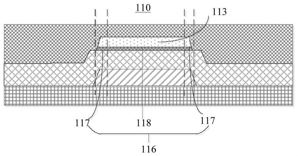
[0035] Figure 2A is a schematic top view structure diagram of the thin film transistor 200 according to the first embodiment of the present invention, Figure 2B for Figure 2A A schematic cross-sectional structure diagram of the middle thin film transistor 200 along the cross-section line C-C'.
[0036] Please also refer to Figure 2A and Figure 2B The thin-film transistor 200 of the bottom gate structure includes a gate 202, an auxiliary layer 203, a gate insulating layer 204, an active layer 205, a source 206, and a drain 207 that are sequentially stacked on a substrate 201, and the active layer 205 includes a The channel region 208 between the source 206 and the drain 207 , the channel region 208 includes an edge region 209 along the channel length direction and a body region 210 except for the edge region 209 . The auxiliary layer 203 is disposed between the gate 202 and the gate insulating layer 204 and is disposed corresponding to the edge region 209 of the channe...
no. 2 example
[0043] image 3 It is a schematic cross-sectional structure diagram of the thin film transistor 200 according to the second embodiment of the present invention. see image 3 The structure of the TFT of the second embodiment of the present invention is basically the same as that of the TFT of the first embodiment, and the only difference lies in the location and material of the auxiliary layer 203 . As shown in the figure, the auxiliary layer 203 is disposed between the active layer 205 and the gate insulating layer 204 . In this embodiment, the auxiliary layer 203 is an auxiliary active layer, and its material is a semiconductor material.
[0044] As shown in the figure, the auxiliary layer 203 is two auxiliary active layers arranged at intervals, and the two auxiliary active layers are respectively arranged corresponding to the two edge regions 209 of the channel region 208 . In another example, the auxiliary layer includes only one auxiliary active layer corresponding to ...
no. 3 example
[0048] Figure 4A is a schematic top view structure diagram of the thin film transistor 200 according to the third embodiment of the present invention, Figure 4B for Figure 4A A schematic cross-sectional structure diagram of the middle thin film transistor 200 along the D-D' section line. For convenience, the same elements are given the same numbers, and will not be described in detail below. Please also refer to Figure 4A and Figure 4B The thin film transistor 200 of the top-gate structure includes a source electrode 206 and a drain electrode 207, an active layer 205, a gate insulating layer 204, an auxiliary layer 203, and a gate electrode 202, which are sequentially stacked on a substrate 201. The active layer 205 includes a The channel region 208 of the gate insulating layer 204 , the channel region 208 includes an edge region 209 along the channel length direction and a body region 210 outside the edge region 209 . The auxiliary layer 203 is disposed between the ...
PUM
| Property | Measurement | Unit |
|---|---|---|
| electron work function | aaaaa | aaaaa |
Abstract
Description
Claims
Application Information
 - R&D
- Intellectual Property
- Life Sciences
- Materials
- Tech Scout
- Unparalleled Data Quality
- Higher Quality Content
- 60% Fewer Hallucinations
Browse by: Latest US Patents, China's latest patents, Technical Efficacy Thesaurus, Application Domain, Technology Topic, Popular Technical Reports.
© 2025 PatSnap. All rights reserved.Legal|Privacy policy|Modern Slavery Act Transparency Statement|Sitemap|About US| Contact US: help@patsnap.com