Supercharge Your Innovation With Domain-Expert AI Agents!

Device and method for cutting crystalline silicon wafer by pulse laser

A technology for cutting crystals and pulsed lasers, which can be used in laser welding equipment, semiconductor devices, electrical components, etc., and can solve problems such as loss of photoelectric conversion efficiency and difficulties

Inactive Publication Date: 2019-03-26
SUZHOU AUTOWAY SYST
View PDF5 Cites 3 Cited by
  • Summary
  • Abstract
  • Description
  • Claims
  • Application Information

AI Technical Summary

Problems solved by technology

However, although the width of the heat-affected zone can reach 100-140um at present, it is very difficult to reach below 110um. For example, polysilicon wafers are generally around 130um. The size of the small heat-affected zone

Method used


Image

  • Device and method for cutting crystalline silicon wafer by pulse laser

Examples


Embodiment Construction

[0018] The present invention will be further described in detail below with reference to the drawings and specific embodiments.

[0019] A method for pulsed laser cutting of crystalline silicon wafers includes the following steps:

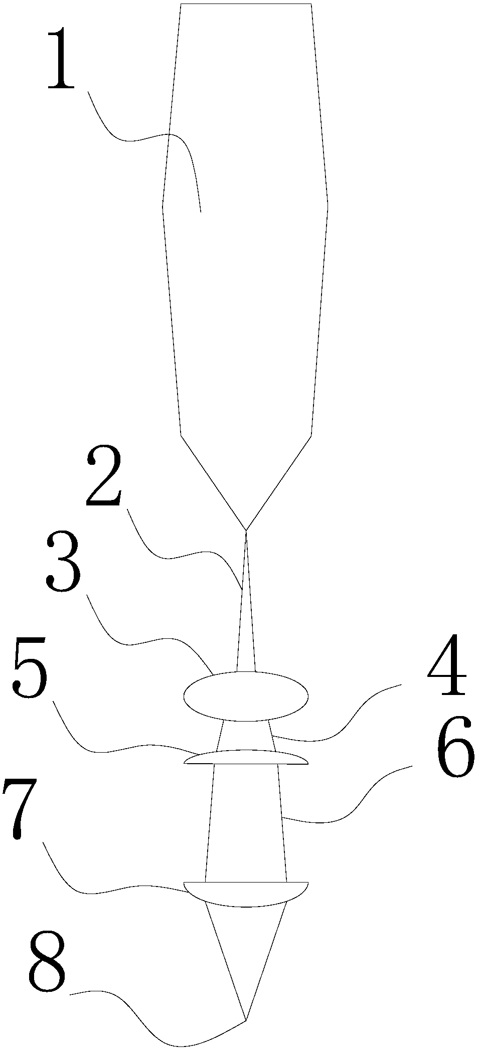
[0020] The step of generating a pulsed laser beam, the pulsed laser spot formed by the pulsed laser beam has two mutually perpendicular axes with different lengths;

[0021] And the step of using the pulsed laser beam to cut the crystalline silicon wafer.

[0022] In the prior art, in the technical field of pulsed laser cutting, efforts are generally made to reduce the converging size (beam size) and pulse laser density of pulsed lasers. The cross-section of pulsed laser beams is circular, and it is used in most materials. In cutting, it is sufficient to meet the above two conditions, so no one thinks about the direction of improvement from other angles (because those skilled in the art have deemed it unnecessary or impossible), but the current technology,...


PUM

PropertyMeasurementUnit
Widthaaaaaaaaaa

Abstract

The invention discloses a device and method for cutting a crystalline silicon wafer by pulse laser. The cross section of a pulse laser beam is creatively adjusted from a circular shape to an elliptical shape, and the long axis direction of the pulse laser beam coincides with or substantially coincides with the cutting direction, so that the size of a heat affected zone of the cutting seam edge iseffectively reduced and contributed to the cutting due to a larger heat diffusion range in the long axis direction, and no effect is caused on cut products.

Description

Technical field [0001] The invention relates to the field of cutting crystalline silicon wafers, in particular to a device and method for cutting crystalline silicon wafers by pulse laser. Background technique [0002] In the field of solar photovoltaics, the production of photovoltaic cells involves the cutting of large quantities of silicon wafers. Cutting is the most widely used processing technology. The principle is that the pulsed laser is focused and irradiated on the material to make the temperature of the material sharp. When it rises to melting or vaporization, with the relative movement of the pulsed laser and the material to be cut, a slit is formed on the material to be cut to achieve the purpose of cutting. Pulsed laser cutting occupies a large proportion in pulsed laser processing applications (currently, pulsed laser cutting accounts for more than 70% of pulsed laser processing), and its application in the photovoltaic industry is becoming more and more extensive....

Claims


Application Information

Patent Timeline
IPC IPC(8): B23K26/38H01L31/18B23K101/40
CPCB23K26/38H01L31/18Y02P70/50
Inventor 唐安伦秦云黄兴俊朱士超鲁乾坤
Owner SUZHOU AUTOWAY SYST
Features
  • R&D
  • Intellectual Property
  • Life Sciences
  • Materials
  • Tech Scout
  • Unparalleled Data Quality
  • Higher Quality Content
  • 60% Fewer Hallucinations
Learn More