A kind of preparation method of nanowire array device

A nanowire array and nanowire technology, which is applied in the field of preparation of nanowire array devices, can solve problems such as process difficulties, and achieve the effect of reducing process difficulty

Active Publication Date: 2020-11-03
CHANGCHUN UNIV OF SCI & TECH
View PDF6 Cites 0 Cited by
  • Summary
  • Abstract
  • Description
  • Claims
  • Application Information

AI Technical Summary

Problems solved by technology

The nanowire array device is prepared by using the nanowire array material fixed by PMMA material, the p-type Ti / Au alloy metal electrode is prepared on the upper surface of the nanowire array material, and the n-type Ni / Au is prepared on the lower surface of the nanowire array material Alloy metal electrodes, n-type and p-type electrodes are prepared by magnetron sputtering technology, after the n-type and p-type electrodes are prepared, the prepared samples are soaked in acetone or toluene solution for 30-60 minutes, and then soaked with alcohol , deionized water for cleaning, and finally allow the sample to dry naturally to obtain a nanowire array device, which solves the difficult problem of obtaining a nanoarray device in the prior art. The method proposed by the present invention is simple to implement and can effectively obtain a nanowire array device

Method used


Image

  • A kind of preparation method of nanowire array device

Examples


Embodiment Construction

[0018] Specific embodiments of the present invention will be described below in conjunction with examples, so as to better understand the present invention.

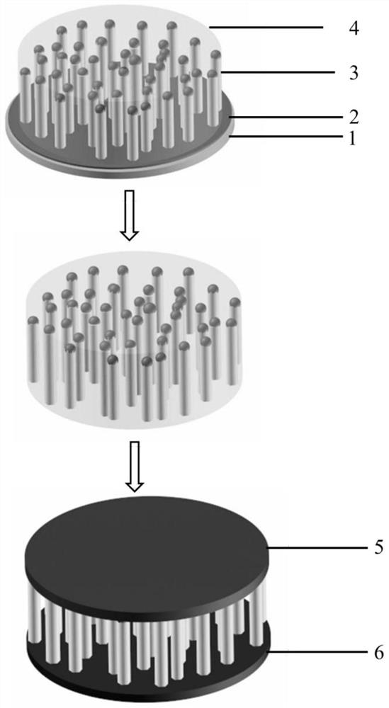
[0019] The invention proposes a method for preparing a nanowire array device. The method first obtains a migratable nanowire array material, and the method for obtaining the nanowire array material is by growing Al on a GaAs substrate. x Ga 1-x As thin film material as sacrificial layer, Al x Ga 1-x The composition of Al in As is 0.6≤x≤1, the nanowire material is grown on Al x Ga 1-x On the As thin film, spin-coat the PMMA material dissolved in acetone solution on the surface of the sample after the growth of the nanowire material and let it dry in the air. At this time, the PMMA material is solidified to fix the nanowire material, and then the nanowire material sample fixed with the PMMA material Put it into the HF acid corrosion solution, use HF acid to Al x Ga 1-x As thin film material has corrosion effect, but ...


PUM

PropertyMeasurementUnit
thicknessaaaaaaaaaa
thicknessaaaaaaaaaa

Abstract

The invention relates to a method for preparing a nanowire array device. The method prepares Al on a substrate for growing nanowires. x Ga 1‑x As thin film was used as sacrificial layer, and nanowires were grown on Al x Ga 1‑x On As, the PMMA material dissolved in acetone solution was used to spin-coat the surface of the nanowire sample to complete the immobilization of PMMA to the nanowire. Put the nanowire sample fixed by PMMA into the HF acid etching solution, and use HF acid to Al x Ga 1‑x As has a corrosive effect, but HF acid has no corrosive effect on GaAs, InAs, and PMMA, so that the Al on the surface of the substrate x Ga 1‑x As is etched away, GaAs nanowires and PMMA materials are completely retained without reacting with HF acid to obtain a migrateable GaAs or InAs nanowire array. Subsequently, a p-type metal electrode is prepared on the upper surface of the migratable nanowire array material, and an n-type metal electrode is prepared on the lower surface. After the electrode preparation is completed, the sample is soaked in acetone or toluene solution to remove PMMA, cleaned and air-dried naturally to obtain The GaAs or InAs nanowire array device solves the problem of technical difficulties in obtaining the nano-array device in the prior art.

Description

technical field [0001] The invention belongs to the field of new materials and novel nano-optoelectronic devices, in particular to a preparation method of a nano-wire array device in the field of nano-optoelectronic materials and devices. Background technique [0002] Nanomaterials are the research hotspots in the world today, and because of their special structure, they are widely used in nano-optoelectronic devices. But because of its unique electrical and optical properties, it can be used to prepare solar cells, optical switches, nano power generation, field effect transistors, light-emitting diodes, nano lasers, photodetectors and other devices, and has been rapidly developed in the fields of nanoelectronics and optoelectronics . Since the ordered array structure membrane battery module was proposed in 2002, the research on the structure based on the ordered array membrane battery module has attracted much attention. Loading the catalyst on the outside of the electron...

Claims


Application Information

Patent Timeline
Patent Type & Authority Patents(China)
IPC IPC(8): B81B7/04B81C1/00
CPCB81B7/04B81C1/00031B81C1/00523
Inventor 贾慧民魏志鹏唐吉龙亢玉彬方铉李洋林逢源王登魁马晓辉
Owner CHANGCHUN UNIV OF SCI & TECH
Why Eureka
Try Eureka