Phase change memory and preparation method thereof

A phase-change memory and phase-change technology, applied in the direction of electric solid devices, semiconductor devices, electrical components, etc., can solve the problems affecting the electrical performance and contact resistance of two-dimensional crystal diodes, and achieve the improvement of electrical performance, storage density, series connection. The effect of low resistance

Inactive Publication Date: 2019-04-02
SHANGHAI INTEGRATED CIRCUIT RES & DEV CENT
View PDF9 Cites 7 Cited by
  • Summary
  • Abstract
  • Description
  • Claims
  • Application Information

AI Technical Summary

Problems solved by technology

However, the two-dimensional crystal material is in contact with any metal, and its contact resistan

Method used


Image

  • Phase change memory and preparation method thereof
  • Phase change memory and preparation method thereof
  • Phase change memory and preparation method thereof

Examples


Embodiment Construction

[0031] In order to make the purpose, technical solution and advantages of the present invention clearer, the specific implementation manners of the present invention will be further described in detail below in conjunction with the accompanying drawings.

[0032] Please refer to the attached Figure 1-6 , the method for preparing phase change memory according to the present invention, specifically comprises the following steps:

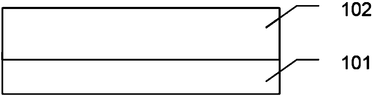
[0033] S01: Please refer to the attached figure 1 A doped layer 102 is formed on the surface of the substrate 101 by ion implantation. Specifically, a conventional P-type Si substrate 101 may be used, and an N-type heavily doped layer 102 is formed on the surface of the P-type Si substrate 101 by ion implantation. In this embodiment, the injection element may be As.

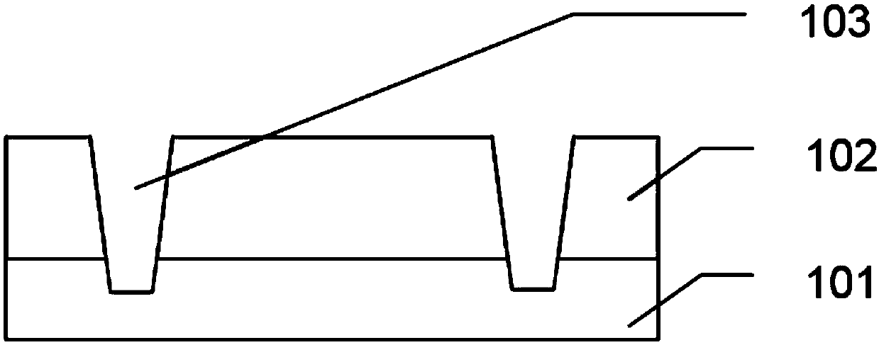
[0034] S02: Please refer to the attached figure 2 A groove 103 is formed in the doped layer and the substrate by photolithography, and the depth of the groove is greater than the de...


PUM


Abstract

The invention discloses a phase change memory, which comprises a substrate, a doping layer, a diode and a phase change resistor from bottom to top, wherein the doping layer is arranged on the top of the substrate; the doping layer and the substrate independently comprise at least two pieces of shallow trench isolation; the diode is positioned between two pieces of shallow trench isolation and comprises a first two-dimensional crystal film and a second two-dimensional crystal film; the second two-dimensional crystal film is positioned above the first two-dimensional crystal film; and the phasechange resistor comprises a lower electrode, sulfide with a phase change ability, and an upper electrode, wherein the lower electrode, the sulfide and the upper electrode are positioned above the second two-dimensional crystal film in sequence. By use of the phase change memory and the preparation method thereof, the unit size of a 1D1R structure phase change memory device unit prepared from the diode prepared from the two-dimensional crystal and the phase change resistor is small, the storage density of the phase change memory can be improved, and meanwhile, graphene is adopted as a lower electrode to lower device power consumption.

Description

technical field [0001] The present invention relates to the field of integrated circuits, in particular to a phase change memory and its preparation method, Background technique [0002] With the emergence of a series of new information technologies such as big data, Internet of Things, cloud computing, and mobile Internet, the requirements for high read / write speed, low power consumption, high storage density, long service life, and high reliability have been put forward for memory. At present, the storage method of memory is mainly DRAM+Flash. NAND Flash has high integration and low cost, but its speed is slow and its lifespan is short. Although DRAM is fast and has a long lifespan, it loses data after power failure and is expensive. Therefore, the research and development of a new type of storage technology has become a research hotspot in the industry in recent years. This type of new storage technology must have the advantages of DRAM and NAND Flash at the same time, t...

Claims


Application Information

Patent Timeline
IPC IPC(8): H01L27/24H01L45/00
CPCH10B63/20H10N70/231H10N70/011
Inventor 钟旻陈寿面李铭
Owner SHANGHAI INTEGRATED CIRCUIT RES & DEV CENT
Why Eureka
Try Eureka