Reproducible manufacturing method for increasing the wavelength of mass-produced MOCVD gallium nitride LED

A manufacturing method and gallium nitride technology, applied in the direction of electrical components, circuits, semiconductor devices, etc., can solve the problems of reduced repeatability of wavelength, achieve the effect of reducing instability and improving repeatability

Inactive Publication Date: 2019-04-05
JIANGSU ZHONGGU OPTO ELECTRONICS
View PDF0 Cites 2 Cited by
  • Summary
  • Abstract
  • Description
  • Claims
  • Application Information

AI Technical Summary

Problems solved by technology

The wavelength of the mass-produced MOCVD (Metal-Organic Chemical Vapor Deposition, metal organic compound chemical vapor deposition) multiple quantum well InGaN / GaN material is related to the width of the well, the growth temperature and the concentration of In, and due to the growth characteristics of the MOCVD machine , the temperature is detected and controlled according to the reflectivity, and is easily affected by other external factors such as the growth substrate and the use of a large plate, resulting in a decrease in the repeatability of the wavelength

Method used


Image

  • Reproducible manufacturing method for increasing the wavelength of mass-produced MOCVD gallium nitride LED
  • Reproducible manufacturing method for increasing the wavelength of mass-produced MOCVD gallium nitride LED
  • Reproducible manufacturing method for increasing the wavelength of mass-produced MOCVD gallium nitride LED

Examples


Embodiment Construction

[0023] Hereinafter, specific implementations of the method for improving the repeatability of the wavelength of the mass-produced MOCVD gallium nitride LED in the present invention will be described in detail with reference to the accompanying drawings, so that the technical content, structural features, objectives and effects of the present invention will be described in detail.

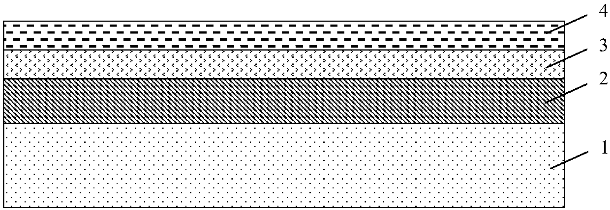
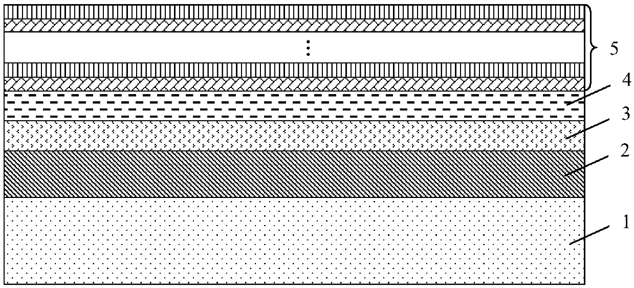
[0024] The present invention provides a method for improving the repeatability of the wavelength of a mass-produced MOCVD gallium nitride LED. The epitaxial structure of the LED includes from bottom to top: Buffer layer, U-GaN layer, N-GaN layer, MQW structure layer, The P-AlGaN layer, the P-GaN layer, and the P+GaN layer specifically include the following steps:

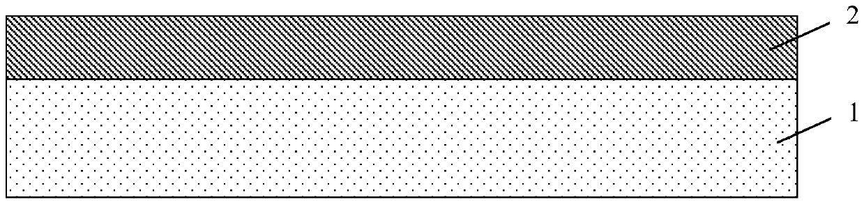
[0025] S1, such as figure 1 As shown, a substrate 1 is provided, and a buffer layer 2 is grown on the substrate 1.

[0026] Wherein, the substrate 1 can be made of any material suitable for the growth of GaN (gallium nitride) and its semiconduc...


PUM


Abstract

The invention relates to a reproducible manufacturing method for increasing the wavelength of a mass-produced MOCVD (Metal-Organic Chemical Vapor Deposition) gallium nitride LED. The method comprisesthe steps of: S1, providing a substrate, and growing a buffer layer on the substrate; S2, growing an undoped GaN layer and an N-GaN layer in order on the buffer layer from top to bottom; S3, growing amulti-quantum well structure layer on the N-GaN layer, wherein the multi-quantum well structure layer is composed of a plurality of sets of periodically stacked grown InGaN layers and GaN layers, inthe process of grown of the InGaN layers, the concentration of In is regulated to a saturated state, and the growth temperature is regulated to modulate the required wavelength of the gallium nitrideLED; S4, growing a P-type electron blocking layer on the multi-quantum well structure layer; S5, growing a P-GaN layer on the P-type electron blocking layer; and S6, growing a P+GaN layer on the P-GaNlayer. The reproducible manufacturing method can effectively reduce the instability and can improve the repeatability of the wavelength.

Description

Technical field [0001] The invention relates to a method for preparing a light emitting diode (LED), in particular to a method for improving the repeatability of the wavelength of a mass-produced MOCVD gallium nitride LED, and belongs to the technical field of semiconductor manufacturing. Background technique [0002] InGaN (indium gallium nitride) is a third-generation material, mainly used in optoelectronic devices and high-temperature, high-frequency, and high-power devices. The InxGa1-xN ternary material can continuously adjust the band gap from 0.7eV (InN) to 3.4eV (GaN) by adjusting the In composition, which can modulate the band from ultraviolet light to near-infrared light. The wavelength of the mass-produced MOCVD (Metal-Organic Chemical Vapor Deposition) multiple quantum well InGaN / GaN material is related to the width of the well, the growth temperature and the In concentration, and due to the growth characteristics of the MOCVD machine , The temperature is controlled ...

Claims


Application Information

Patent Timeline
Patent Type & Authority Applications(China)
IPC IPC(8): H01L33/00H01L33/06H01L33/32
CPCH01L33/0075H01L33/06H01L33/325
Inventor 任朝花
Owner JIANGSU ZHONGGU OPTO ELECTRONICS
Why Eureka
Try Eureka