
An all-inorganic lead halide perovskite light-emitting diode and its preparation method and active light-emitting layer

A light-emitting diode and lead halide technology, which is applied in the fields of organic semiconductor devices, semiconductor/solid-state device manufacturing, electric solid-state devices, etc., can solve the problem of poor stability of perovskite light-emitting diodes and easy oxidation into tetravalent tin ions and divalent tin Ion instability and other issues, to achieve the effect of film morphology improvement, fluorescence intensity improvement, not easy to oxidative denaturation

Active Publication Date: 2022-04-29
SUZHOU UNIV
View PDF4 Cites 0 Cited by
  • Summary
  • Abstract
  • Description
  • Claims
  • Application Information

AI Technical Summary

Problems solved by technology

However, tin-based perovskite light-emitting diodes suffer from poor stability and low efficiency.
Because divalent tin ions are very unstable and are easily oxidized to tetravalent tin ions, which leads to the instability of the perovskite structure

Method used


Image

  • An all-inorganic lead halide perovskite light-emitting diode and its preparation method and active light-emitting layer
  • An all-inorganic lead halide perovskite light-emitting diode and its preparation method and active light-emitting layer
  • An all-inorganic lead halide perovskite light-emitting diode and its preparation method and active light-emitting layer

Examples


Embodiment example 1

[0054] Preparation of active light-emitting layer precursors containing alkaline earth metal bromides: MgBr 2 , CsBr and PbBr 2 Dissolved in DMSO, CsBr, MgBr in the active light-emitting layer precursor 2 and PbBr 2 The molar ratio is 1:0.05:0.95, and the concentration is 0.2M.

[0055] TFB was dissolved in chlorobenzene to obtain a first hole transport layer solution with a concentration of 8 mg / ml.

[0056] PVK was dissolved in toluene to obtain a second hole transport layer solution with a concentration of 4 mg / ml.

[0057] The solution prepared above was heated and stirred at 50° C. for 2 hours, and then used.

[0058] The ITO transparent substrate was ultrasonically cleaned with acetone, ethanol, and deionized water for 20 minutes, dried with nitrogen, and then treated with oxygen plasma for 15 minutes. The substrate was placed in a nitrogen glove box to prepare the device.

[0059] Preparation of the hole transport layer: first, the first hole transport layer soluti...

Embodiment example 2

[0066] MgBr 2 , CsBr and PbBr 2 Dissolved in DMSO to prepare an active light-emitting layer precursor containing alkaline earth metal bromide, the active light-emitting layer precursor contains CsBr, MgBr 2 and PbBr 2 The molar ratio is 1:0.1:0.9, and the concentration is 0.2M.

[0067] TFB was dissolved in chlorobenzene to obtain a first hole transport layer solution with a concentration of 8 mg / ml.

[0068] PVK was dissolved in toluene to obtain a second hole transport layer solution with a concentration of 4 mg / ml.

[0069] The solution prepared above was heated and stirred at 50° C. for 2 hours, and then used.

[0070] The ITO transparent substrate was ultrasonically cleaned with acetone, ethanol, and deionized water for 20 minutes, dried with nitrogen, and then treated with oxygen plasma for 15 minutes. The substrate was placed in a nitrogen glove box to prepare the device.

[0071] Preparation of the hole transport layer: first, the first hole transport layer soluti...

Embodiment example 3

[0078] MgBr 2 , CsBr and PbBr 2 Dissolved in DMSO to prepare an active light-emitting layer precursor containing alkaline earth metal bromide, the active light-emitting layer precursor contains CsBr, MgBr 2 and PbBr 2 The molar ratio is 1:0.2:0.8, and the concentration of the precursor solution is 0.2M.

[0079] TFB was dissolved in chlorobenzene to obtain a first hole transport layer solution with a concentration of 8 mg / ml.

[0080] PVK was dissolved in toluene to obtain a second hole transport layer solution with a concentration of 4 mg / ml.

[0081] The solution prepared above was heated and stirred at 50° C. for 2 hours, and then used.

[0082] The ITO transparent substrate was ultrasonically cleaned with acetone, ethanol, and deionized water for 20 minutes, dried with nitrogen, and then treated with oxygen plasma for 15 minutes. The substrate was placed in a nitrogen glove box to prepare the device.

[0083]Preparation of the hole transport layer: first, the first ho...


PUM

PropertyMeasurementUnit
thicknessaaaaaaaaaa
thicknessaaaaaaaaaa
thicknessaaaaaaaaaa

Abstract

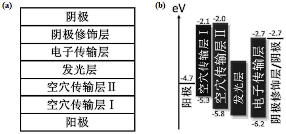
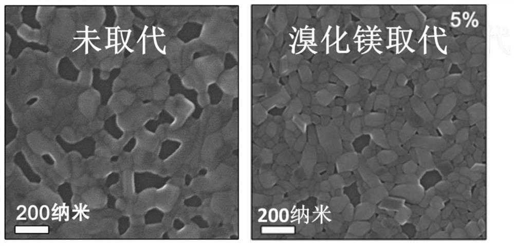
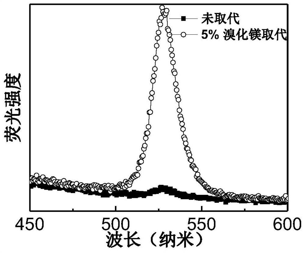
The invention discloses an all-inorganic lead halide perovskite light-emitting diode, which comprises a conductive substrate, a carrier transport layer, an electrode modification layer and an electrode sequentially arranged in a layered structure, wherein the carrier transport layer is arranged in the middle The active luminescent layer is a lead halide perovskite in which part of the lead halide is replaced by an alkaline earth metal halide. In this application, part of the lead halide in the perovskite is replaced by alkaline earth metal. On the one hand, the formation energy of the bromine defect state in the perovskite becomes higher, which means that the bromine defect is more difficult to form, so the defect state of the perovskite is significantly reduced and the fluorescence is enhanced. On the other hand, the morphology of the film is significantly improved, the pores are reduced, and the leakage current is reduced. At the same time, due to the enhanced fluorescence, the brightness is improved, and finally the efficiency of the entire device is improved.

Description

technical field [0001] The invention relates to the field of photoelectric devices, in particular to an all-inorganic lead halide perovskite light-emitting diode and a preparation method thereof. Background technique [0002] In recent years, perovskite materials have been widely used in display and other fields due to their excellent photoelectric properties, pure chromaticity, and adjustable bandgap width. At present, the external quantum efficiency of thin-film perovskite light-emitting diodes based on pure lead has exceeded 20%, which is comparable to traditional organic light-emitting diodes and quantum dot light-emitting diodes. However, due to the strong toxicity of lead ions, it will cause great harm to the human body and the environment, which greatly inhibits the application of this type of perovskite light-emitting diodes. In order to meet the requirements of commercialization of perovskite devices, we need to find other non-toxic metal elements to replace the to...

Claims


Application Information

Patent Timeline
Patent Type & Authority Patents(China)
IPC IPC(8): H01L51/54H01L51/50H01L51/56
CPCH10K71/00H10K50/11H10K2102/00
Inventor 孙宝全宋涛黄琪
Owner SUZHOU UNIV
Learn More