3D stacked image sensor
An image sensor and pixel array technology, applied in image communication, electric solid-state devices, semiconductor devices, etc., can solve the problems of not greatly improving the frame rate, limited chip area, slow data transmission speed, etc., to improve the frame rate, The effect of simple manufacturing process
- Summary
- Abstract
- Description
- Claims
- Application Information
AI Technical Summary
Problems solved by technology
Method used
Image

Examples
Embodiment Construction
[0021] In order to make the content of the present invention clearer and easier to understand, the content of the present invention will be further described below in conjunction with the accompanying drawings. Of course, the present invention is not limited to this specific embodiment, and general replacements known to those skilled in the art are also covered within the protection scope of the present invention.
[0022] The following is attached Figure 2-7 The present invention will be described in further detail with specific examples. It should be noted that the drawings are all in a very simplified form, using imprecise scales, and are only used to facilitate and clearly achieve the purpose of assisting in describing the present embodiment.
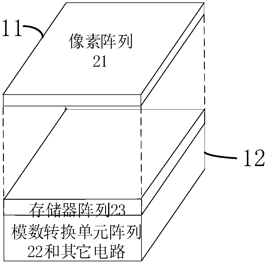
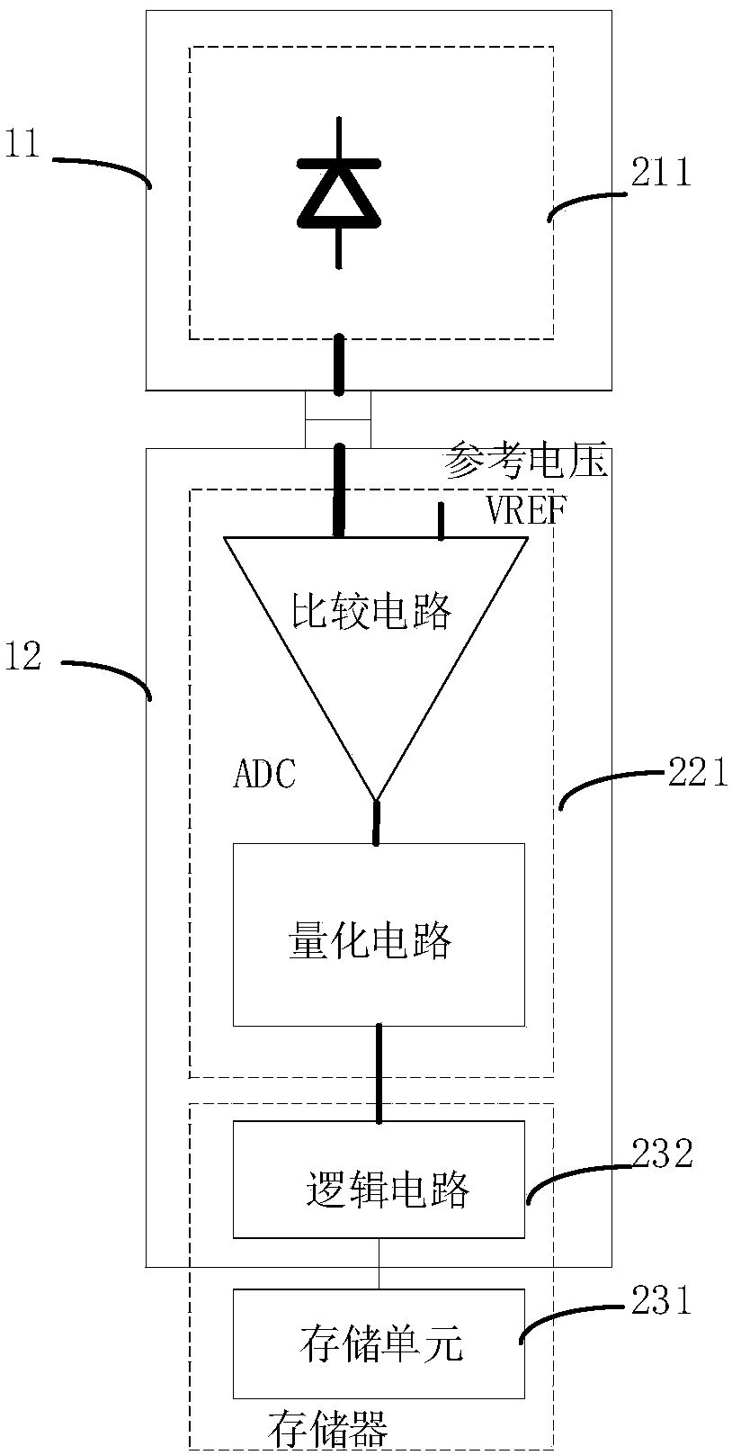
[0023] refer to figure 2 , image 3 with Figure 4 , figure 2 Shown is a schematic structural diagram of a 3D stacked image sensor according to an embodiment of the present invention, image 3 Shown is a schematic diagram o...
PUM
 Abstract
Description
Claims
Application Information