
Semiconductor packaging mold, semiconductor device and packaging method for semiconductor device

A packaging method and semiconductor technology, applied in semiconductor devices, semiconductor/solid-state device parts, semiconductor/solid-state device manufacturing, etc., can solve problems such as peeling of packaging materials and chips, and warping of packaging materials or chips. Small, the effect of reducing the possibility of peeling

Active Publication Date: 2020-08-18
SEMICON MFG INT (SHANGHAI) CORP +1
View PDF2 Cites 0 Cited by
  • Summary
  • Abstract
  • Description
  • Claims
  • Application Information

AI Technical Summary

Problems solved by technology

[0003] Packaging is carried out using the packaging mold in the prior art. After the heat treatment makes the packaging material solidify, the packaging material or chip is prone to warping, resulting in peeling between the packaging material and the chip, and the chip cannot be effectively packaged and protected.

Method used


Image

  • Semiconductor packaging mold, semiconductor device and packaging method for semiconductor device
  • Semiconductor packaging mold, semiconductor device and packaging method for semiconductor device
  • Semiconductor packaging mold, semiconductor device and packaging method for semiconductor device

Examples


no. 1 example

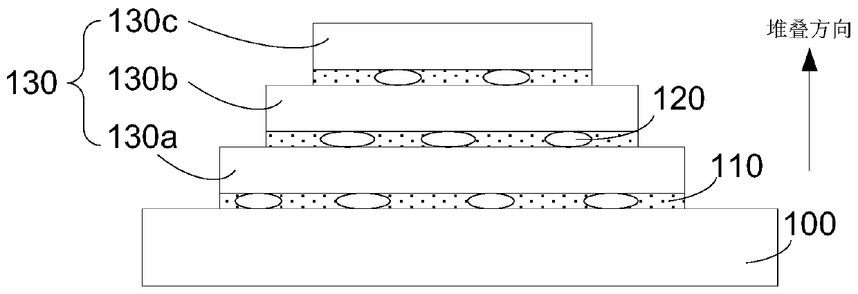
[0051] Please refer to figure 1 , a plurality of chips 130 are stacked on the packaging substrate 100.

[0052] The packaging substrate 100 functions to support and protect the chip 130 . The material of the packaging substrate 100 includes, but is not limited to: epoxy resin, polyimide, and the like. Specifically, in the embodiment of the present invention, the material of the packaging substrate 100 is epoxy resin.

[0053] The shape of the chip 130 is square, circular, etc., and there is no specific limitation here. Specifically, in the embodiment of the present invention, the shape of the chip 130 is square. The base material of chip 130 is silicon.

[0054] Each chip 130 includes opposite first and second surfaces. Specifically, in the embodiment of the present invention, the first surface refers to the top surface of each chip 130 , and the second surface refers to the bottom surface of each chip 130 .

[0055] It should be noted that there is no specific limitati...

no. 2 example

[0089] The difference between the second embodiment and the first embodiment lies in that the outline shape of the chip receiving cavity of the packaging mold is different, and the other parts and the positional relationship between the parts are consistent with the first embodiment.

[0090] Please refer to Figure 5 , cover the stacked chips 230 with the packaging mold 240 .

[0091] Functions and positional relationships of the packaging substrate 200 , the metal interconnection structure 210 , and the filling material 220 are consistent with those of the first embodiment, and will not be repeated here.

[0092] Please refer to the first embodiment for the shape, stacking method, positional relationship, and width dimension of the chips 230 .

[0093] The encapsulation mold 240 covers the stacked chips 230 for subsequent filling of encapsulation material. The chip receiving cavity accommodates all the chips 230 , and the profile of the chip receiving cavity of the packagi...

no. 3 example

[0120] The difference between the third embodiment and the second embodiment lies in the outline shape of the chip containing cavity of the packaging mold and the stacking manner of the chips. One side of the cross-sectional profile shape of the packaging mold chip accommodation cavity in the depth direction is a plane, and at the same time, one side of all the stacked chips is kept flush. For the functions and positional relationships of other components of the third embodiment, please refer to the second embodiment.

[0121] Please refer to Figure 9 , a plurality of chips 330 are stacked on the packaging substrate 300 .

[0122] The functions and materials of the packaging substrate 300 are consistent with those of the second embodiment, and will not be repeated here.

[0123] Chips 330 are stacked on the package substrate 300 . The functions of stacking the chips 330 , the connection methods between different chips 330 and between the chips 330 and the package substrate...


PUM

PropertyMeasurementUnit
thicknessaaaaaaaaaa
thicknessaaaaaaaaaa

Abstract

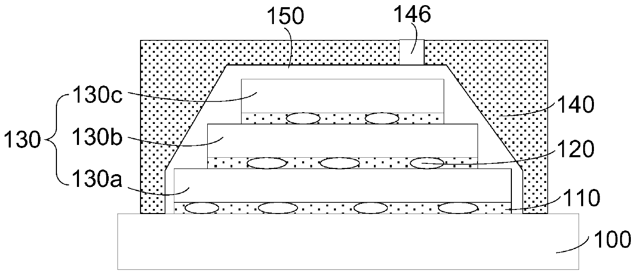
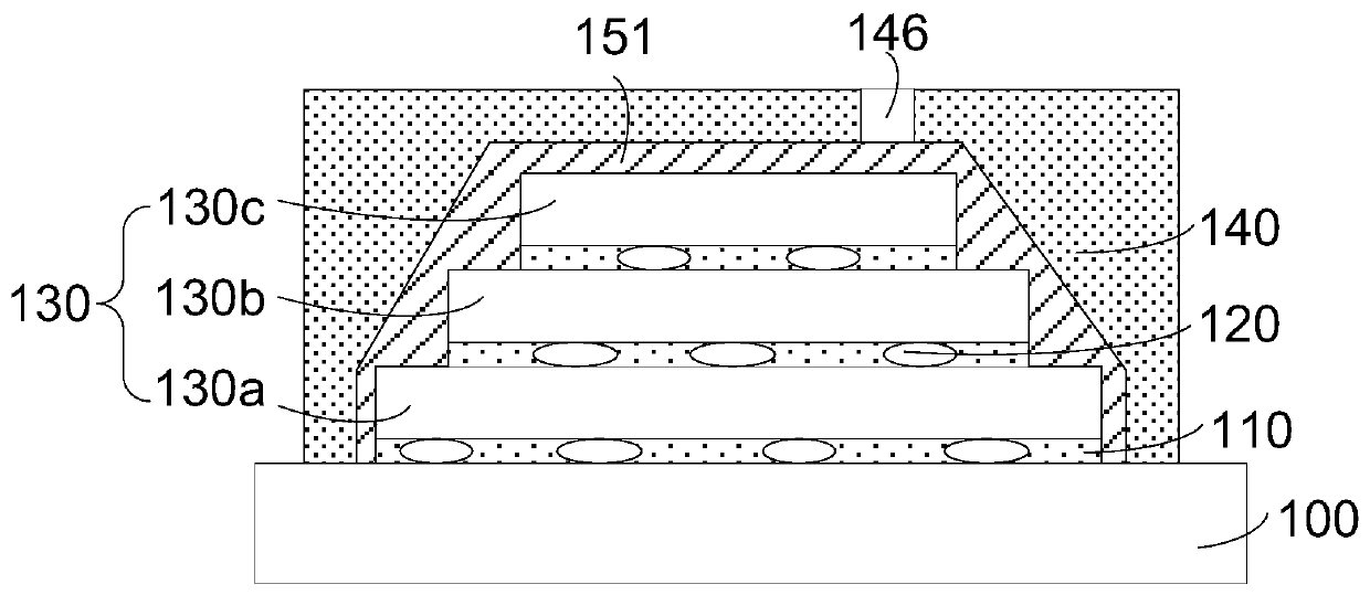
The invention discloses a semiconductor packaging mold, a semiconductor device and a packaging method for the semiconductor device. The semiconductor packaging method includes providing a packaging substrate on which a plurality of chips are stacked; covering the chip with a packaging mold so that the chip accommodation cavity accommodates all the chips, and the outline surface shape of the chip accommodation cavity is adapted to the outline surface shape of the stacked chips; The encapsulation material is injected into the chip accommodation cavity through the injection hole. The fit of the chip accommodation chamber to the outer contour surface of the stacked chips makes the subsequently formed packaging material thinner and uniform in thickness, avoiding warping of the chip and the packaging material.

Description

technical field [0001] The invention relates to the field of semiconductor manufacturing, in particular to a semiconductor packaging mold, a semiconductor device and a packaging method for the semiconductor device. Background technique [0002] At present, in the process of chip packaging, the emergence of 3D stacking of chips reduces the area occupied by the two-dimensional arrangement of chips. 3D stacking is to place chip stacks on packaging substrates and then package them. In the prior art, a packaging mold with a single square chip receiving cavity is used to cover the stacked chip structure, and then packaged. [0003] Packaging is carried out using the packaging mold in the prior art. After the packaging material is cured by heat treatment, the packaging material or the chip is prone to warping, resulting in peeling between the packaging material and the chip, and the chip cannot be effectively packaged and protected. [0004] Therefore, there is an urgent need in ...

Claims


Application Information

Patent Timeline
Patent Type & Authority Patents(China)
IPC IPC(8): H01L21/56H01L23/31
CPCH01L21/565H01L23/3114H01L23/3121H01L2224/16145H01L2224/32145H01L2224/32225H01L2224/16225H01L2224/73204H01L2924/00
Inventor 陈彧
Owner SEMICON MFG INT (SHANGHAI) CORP
Learn More