Display panel and manufacturing method thereof

A display panel and manufacturing method technology, applied in the direction of electrical components, electrical solid devices, circuits, etc., can solve the problems of short lifespan, reduced lifespan, and low light transmittance of light-emitting organic materials in OLED displays, so as to reduce the metal annealing process and reduce the conductivity. The effect of high on-resistance and light transmittance

Active Publication Date: 2019-04-16
WUHAN CHINA STAR OPTOELECTRONICS SEMICON DISPLAY TECH CO LTD
View PDF4 Cites 4 Cited by
  • Summary
  • Abstract
  • Description
  • Claims
  • Application Information

AI Technical Summary

Problems solved by technology

The current contact methods and materials are as follows: the contact between the semiconductor layer (P-Si) and the source and drain (Ti / Al / Ti) is a metal-semiconductor contact, and the resistance is large; the anode (ITO / Ag / ITO) and the source and drain (Ti / Al / Ti) / Al / Ti) contact requires a metal annealing process, but there is also a corresponding contact resistance
In addition, the ITO (Indium Tin Oxide) film on the upper layer of the anode is an amorphous film, which causes problems of low light transmittance and high resistance, and the photons and electrical energy in the ITO film are converted into heat energy, and the life of the OLED display light-emitting organic matter itself Short, so the life expectancy will drop sharply in high temperature environment

Method used


Image

  • Display panel and manufacturing method thereof
  • Display panel and manufacturing method thereof
  • Display panel and manufacturing method thereof

Examples


Embodiment Construction

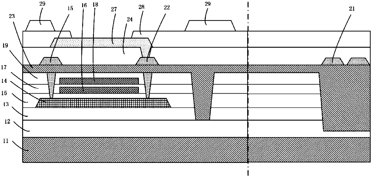
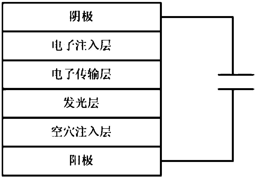
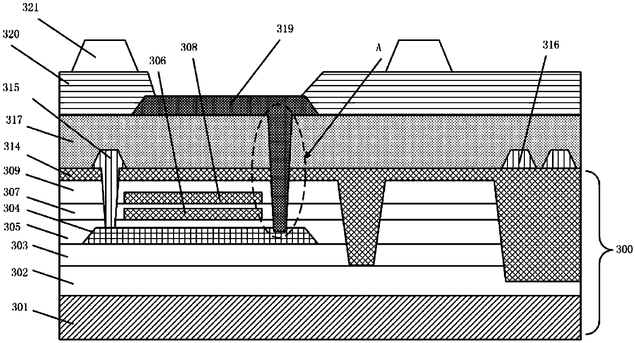
[0026] The following will clearly and completely describe the technical solutions in the embodiments of the present invention with reference to the drawings in the embodiments of the present invention. Apparently, the described embodiments are only some of the embodiments of the present invention, but not all of them. Based on the embodiments of the present invention, all other embodiments obtained by those skilled in the art without creative efforts fall within the protection scope of the present invention.

[0027] The terms "first", "second", "third", etc. (if any) in the description and claims of the present invention and the above drawings are used to distinguish similar objects and not necessarily to describe a specific order or sequentially. It should be understood that the items so described are interchangeable under appropriate circumstances. Furthermore, the terms "comprising" and "having", as well as any variations thereof, are intended to cover a non-exclusive in...


PUM


Abstract

The invention discloses a display panel and a manufacturing method thereof. In the display panel, an anode and a drain are integrated so as to avoid contact resistance between the anode and the drain,thereby reducing a metal annealing process. Moreover, the anode is made of a zinc oxide material superior to ITO in resistivity and light transmittance and easy to be subsequently etched, thereby reducing the on-resistance of the display panel and increasing the light reflection of the anode.

Description

technical field [0001] The invention relates to the field of display technology, in particular to a display panel and a manufacturing method thereof. Background technique [0002] Flat panel display technologies such as Liquid Crystal Display (LCD) and Organic Light Emitting Diode (OLED) have gradually replaced CRT displays. Among them, OLED displays have many advantages such as self-illumination, low driving voltage, high luminous efficiency, short response time, high definition and contrast, nearly 180° viewing angle, wide operating temperature range, flexible display and large-area full-color display, etc. It is recognized by the industry as the most promising display device. [0003] The OLED display panel is an important part of the OLED display. Such as figure 1 As shown, the OLED display panel generally includes: a base substrate (including a PI film layer 11, a barrier layer 12, and a buffer layer 13), a plurality of thin film transistors (Thin Film transistors) a...

Claims


Application Information

Patent Timeline
Patent Type & Authority Applications(China)
IPC IPC(8): H01L27/32
CPCH10K59/123H10K59/12H10K59/1213H10K50/818H10K59/1201
Inventor 张伟彬
Owner WUHAN CHINA STAR OPTOELECTRONICS SEMICON DISPLAY TECH CO LTD
Why Eureka
Try Eureka