
Method for low-voltage assistance in connection of nano silver solder paste with large-area substrate and heat dissipating device

A heat sink, nano-silver technology, applied in nanotechnology, nanotechnology, nanotechnology for materials and surface science, etc., can solve the problems of organic residues, affecting the thermal conductivity and reliability of sintered substrates, and save sintering costs. , the effect of low elastic modulus and excellent thermal conductivity

Inactive Publication Date: 2019-04-19
TIANJIN UNIV
View PDF2 Cites 0 Cited by
  • Summary
  • Abstract
  • Description
  • Claims
  • Application Information

AI Technical Summary

Problems solved by technology

The disadvantage of this type of sintering process is that after using wet nano-silver solder paste to contact the two substrates, a large amount of liquid organic matter exists in the solder paste. During the closed drying process, the organic matter is difficult to volatilize completely, and a large amount of organic matter remains. When the boiling point of the residual organic matter is higher than the boiling point of the residual organic matter, the liquid organic matter boils, and the solder paste is not completely dry at this time, so there are voids and cracks in the spreading area, which seriously affect the thermal conductivity and reliability of the sintered substrate
[0005] The above two processes have their own advantages and disadvantages

Method used


Image

  • Method for low-voltage assistance in connection of nano silver solder paste with large-area substrate and heat dissipating device
  • Method for low-voltage assistance in connection of nano silver solder paste with large-area substrate and heat dissipating device
  • Method for low-voltage assistance in connection of nano silver solder paste with large-area substrate and heat dissipating device

Examples


Embodiment Construction

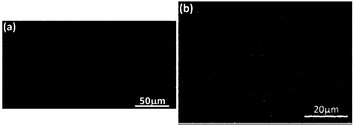
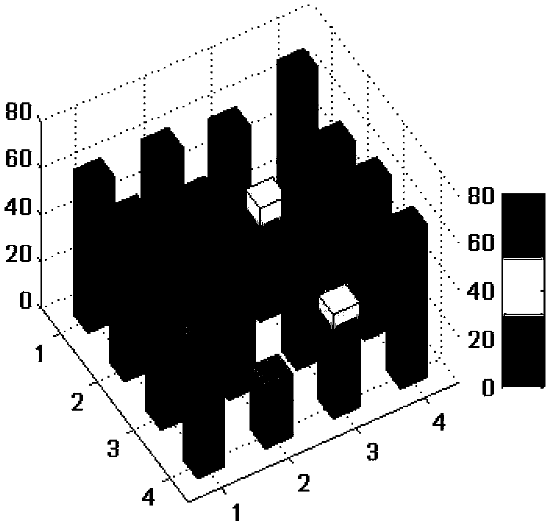
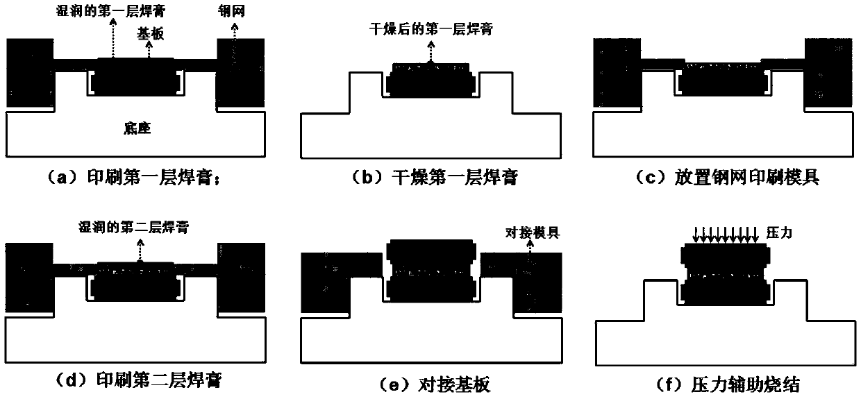
[0026] Such as figure 1 Shown is the manufacturing process of the method for connecting a large-area substrate and a heat sink with a low-pressure assisted nano-silver solder paste. Such as figure 2 Shown is the sintering process curve of the low-pressure assisted nano-silver solder paste connecting the large-area substrate and the heat sink. Combine below figure 1 and figure 2 The specific sintering process of low-voltage assisted nano-silver solder paste connecting large-area substrates and heat sinks is described in detail:

[0027] (1) The pretreatment process is as follows: 99.9% copper substrate is used, and the substrate area is greater than 800mm 2 , cut into 25.4mm*45.72mm*1mm, and electroplate a 10μm silver layer after cleaning; clean the silver-plated copper substrate in an ultrasonic cleaner for 10 minutes, and wipe it with a dust-free paper after cleaning;

[0028] (2) Put the cleaned substrate on the base of the mold, and fix the steel mesh matching the ba...


PUM

PropertyMeasurementUnit
Thicknessaaaaaaaaaa
Areaaaaaaaaaaa
Shear strengthaaaaaaaaaa

Abstract

The invention discloses a method for low-voltage assistance in connection of a nano silver solder paste with a large-area substrate and a heat dissipating device. The method is specifically for the connection between a large-area substrate having a substrate area of more than 800 mm2 and a heat dissipating device (a heat dissipating bottom plate, a heat sink, etc.). The purpose of employing a double-layer printing nano silver solder paste process is to ensure that the second layer of nano silver solder paste is relatively thin to ensure sufficient contact between the wet nano silver solder paste and another substrate and make the content of the organic content not excessive so as to facilitate volatilization of organic matter in the subsequent sintering process. Innovative introduction of'fast drying process (from 65-85 DEG C / min to room temperature to 160-180 DEG C) ', after the rapid drying process, the nano-silver solder paste layer has no cracks and uses a small pressure (1MPa-5MPa) to allow the nano silver solder paste layer structure to have a dense structure and a high bonding strength.

Description

technical field [0001] The invention relates to a low-pressure (pressure lower than 5MPa) assisted nano-silver solder paste to connect large areas (bonding area greater than 800mm) 2 ) The sintering method of the substrate, the heat dissipation bottom plate, the heat sink, etc. belongs to a new packaging method for applying the nano-silver solder paste of the new thermal interface material to the high-power electronic power packaging system. Background technique [0002] During the working process of semiconductor devices, a large amount of heat will be generated in local areas, and the heat needs to be conducted out in a timely and effective manner to ensure the normal operation of semiconductor devices. For high-temperature and high-power electronic power packaging systems, heat dissipation is a key issue that determines the efficiency and reliability of the entire system. The thermal interface material can effectively fill the air gap between the substrate and the coolin...

Claims


Application Information

Patent Timeline
IPC IPC(8): H01L21/48B82Y30/00
CPCH01L21/4882B82Y30/00H01L23/3735H01L23/3736
Inventor 陈旭谭延松李欣
Owner TIANJIN UNIV
Learn More