

High-speed digital logic circuit for SAR_ADC and sampling regulation method
A digital logic circuit, high-speed technology, applied in the direction of logic circuits, electrical components, analog-to-digital converters, etc., can solve the problems of increasing the difficulty of circuit design and increasing design costs, and achieve the effect of increasing the adoption time and improving the sampling accuracy
- Summary
- Abstract
- Description
- Claims
- Application Information
AI Technical Summary
Problems solved by technology
Method used
Image

Examples
Embodiment 1
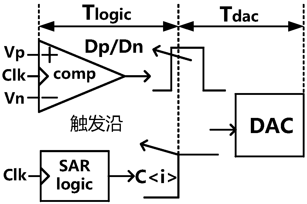
[0028] This embodiment is explained by taking a 10-bit SAR structure ADC as an example, that is, N=10; the schematic diagram of the parallel SARlogic used in the present invention is as follows image 3 shown. The comparator comp and the logic control unit SAR logic are simultaneously triggered by the signal Clk, after a delay, the comparator outputs the effective comparison result Dp / Dn, and the SAR logic outputs the corresponding rising edge signal C (i=0,1,…,9), by setting an appropriate delay, the rising edge signal C output by SAR logic (i=0,1,…,9) a little later than the comparator outputs the effective comparison result Dp / Dn, so that Dp / Dn is detected by the corresponding rising edge signal C (i=0,1,...,9) capture.
[0029] In the present invention, due to the rising edge signal C (i=0, 1, . . . , 9) is later than the comparator to output an effective comparison result Dp / Dn, so that the capacitor array will not be incorrectly established, and the accuracy of t...
Embodiment 2
[0040] The present invention also proposes a sampling time adjustment method, that is, a sampling adjustment method for a high-speed digital logic circuit of SAR_ADC. After 10 successive approximation processes are completed, the external sampling control signal Clks is still 0, and the eleventh D flip-flop The generated output signal CO becomes 1, so that the output of the OR gate OR is Clks_in becomes 1, so that SAR_ADC immediately enters the sampling state, and at the same time, the first 10 D flip-flops are reset. When the external sampling control signal Clks changes from 0 to 1, the 11th D flip-flop is reset, and its output signal CO becomes 0. Since the external sampling control signal Clks is 1 at this time, the output signal Clks_in of the OR gate is still Keep it as 1, so that SAR_ADC is still in the sampling state, until the external sampling control signal Clks becomes 0, the sampling state ends, and SAR_ADC enters the successive approximation state.
[0041] A...
Embodiment 3
[0043] In order to further verify the above-mentioned advantages of the present invention, the above-mentioned structure is carefully designed under the 65nm CMOS process, and the power supply voltage is 1.2V. Adopt above-mentioned three kinds of structures (comprising traditional asynchronous SAR logic, traditional parallel asynchronous SAR logic and SAR logic proposed by the present invention) to design a 10-bit 100MHz sampling rate SAR_ADC respectively, through simulation result, the conversion time and sampling time of above-mentioned three kinds of structures are carried out Compared. Set the external sampling time of the three structures to 1ns, and the average delay comparison of the successive approximation process of the three structures is as follows Figure 7 shown by Figure 7 It can be seen that, compared with the traditional asynchronous SARlogic, the present invention has improved the speed by at least 37.5%. Compared with the parallel asynchronous SAR logi...
PUM
 Abstract
Description
Claims
Application Information