Method for large-area preparation of two-dimensional molybdenum telluride in-plane heterojunction with contact of metal phase and semiconductor phase and application thereof

A technology for semiconductors and molybdenum telluride, which is applied in the large-area preparation of two-dimensional molybdenum telluride in-plane heterojunctions in which the metal phase and the semiconductor phase are in contact and the application field can solve problems such as inability to produce large-scale, achieve low contact resistance, Effects of improving electrical performance and improving injection efficiency

Active Publication Date: 2019-05-07
PEKING UNIV
View PDF9 Cites 12 Cited by
  • Summary
  • Abstract
  • Description
  • Claims
  • Application Information

AI Technical Summary

Problems solved by technology

However, the current methods to realize this structure mainly use some processes that cannot be prepared on a large scale, and are limited to the preparation of a single device. Therefore

Method used


Image

  • Method for large-area preparation of two-dimensional molybdenum telluride in-plane heterojunction with contact of metal phase and semiconductor phase and application thereof
  • Method for large-area preparation of two-dimensional molybdenum telluride in-plane heterojunction with contact of metal phase and semiconductor phase and application thereof
  • Method for large-area preparation of two-dimensional molybdenum telluride in-plane heterojunction with contact of metal phase and semiconductor phase and application thereof

Examples


Embodiment Construction

[0023] The present invention will be further elaborated below through specific implementation examples in conjunction with the accompanying drawings.

[0024] In this embodiment, the method for preparing a large-area in-plane heterojunction of molybdenum telluride with a metal phase in contact with a semiconductor phase includes the following steps:

[0025] 1) Provide a substrate, the substrate includes a lower conductive layer and an upper insulating layer, the lower layer is heavily doped p-type Si, and the upper layer is SiO 2 , SiO 2 The thickness is 285nm.

[0026] 2) A molybdenum thin film with a thickness of about 2 nanometers is vapor-deposited on the substrate by magnetron sputtering.

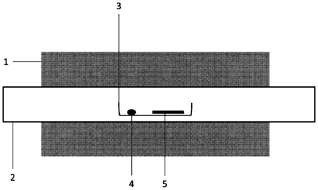
[0027] 3) see figure 1 , put the tellurium powder 4 and the substrate 5 steamed with a molybdenum thin film into the quartz boat 3, and then place them into the quartz tube 2 of the tube furnace 1. After 15 minutes of heating up, the temperature zone of the tube furnace is heated ...


PUM


Abstract

The invention discloses a method for large-area preparation of two-dimensional molybdenum telluride in-plane heterojunction with contact of a metal phase and a semiconductor phase and application thereof. The method comprises the steps of: growing a two-dimensional molybdenum thin film on a substrate, employing a chemical vapor deposition method to convert the two-dimensional molybdenum thin filmto a semiconductor phase molybdenum telluride thin film, performing photolithography and etching imaging of the semiconductor phase molybdenum telluride thin film, growing a molybdenum thin film, performing peeling to obtain a thin film with spaced apart metal phases and semiconductor phase molybdenum telluride, and further employing the chemical vapor deposition method to convert the metal molybdenum thin film to a metal phase molybdenum telluride thin film to obtain a two-dimensional molybdenum telluride in-plane heterojunction with contact of the metal phase and the semiconductor phase. Thefield effect transistor array of the two-dimensional molybdenum telluride in-plane heterojunction with contact of the metal phase and the semiconductor phase is low in contact resistance, improves the injection efficiency of the carrier, and improves the electrical properties of the device. The method provides basis for application of the two-dimensional semiconductor materials at the aspects ofintegration circuits and flexible devices.

Description

technical field [0001] The invention relates to the preparation of a thin-film transistor based on a two-dimensional material, in particular to a large-area method and application for preparing a thin-layer molybdenum telluride in-plane heterojunction in which a two-dimensional metal phase and a semiconductor phase are in contact. Background technique [0002] With the development of integrated circuits, the traditional silicon-based complementary metal-oxide-semiconductor field-effect transistor technology has approached its physical limit, and new materials are needed to continue Moore's law. Two-dimensional semiconductor materials can effectively suppress the short channel effect caused by the reduction of device channel size due to its characteristic of only one or several atomic layer thickness. However, due to the lack of dangling bonds on the surface of the two-dimensional semiconductor material, a tunneling layer will be formed between the traditional metal electrode...

Claims


Application Information

Patent Timeline
IPC IPC(8): H01L21/02H01L29/06H01L29/778
Inventor 徐晓龙叶堉戴伦
Owner PEKING UNIV
Why Eureka
Try Eureka