Spin memory and calculation integrated chip

A chip and integrated technology, applied in the field of spin-memory-computing integrated chips, can solve the problems of low integration, large static power consumption of massive data, etc., to achieve the effect of improving stability, suitable for large-scale promotion and use, and low storage power consumption

Active Publication Date: 2019-05-17
致真存储(北京)科技有限公司
View PDF5 Cites 23 Cited by
  • Summary
  • Abstract
  • Description
  • Claims
  • Application Information

AI Technical Summary

Problems solved by technology

[0008] The existing SRAM-based integrated storage and computing technology still has problems such as high static power consumption and low integration for solving the transmission and processing of ma...

Method used


Image

  • Spin memory and calculation integrated chip
  • Spin memory and calculation integrated chip
  • Spin memory and calculation integrated chip

Examples


Embodiment 1

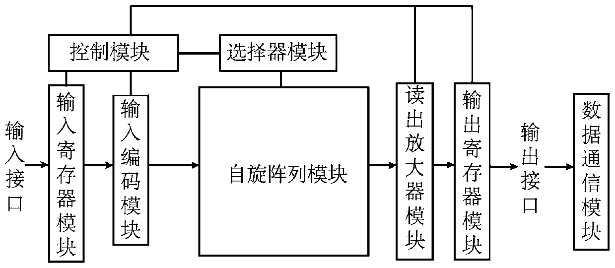
[0071] The embodiment of the present invention discloses a spin-storage-computing integrated chip, such as figure 1 As shown, including: spin array module and peripheral circuits;

[0072] The spin array module is connected with peripheral circuits;

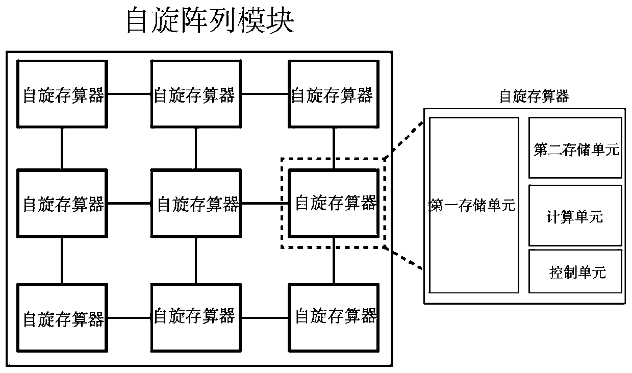
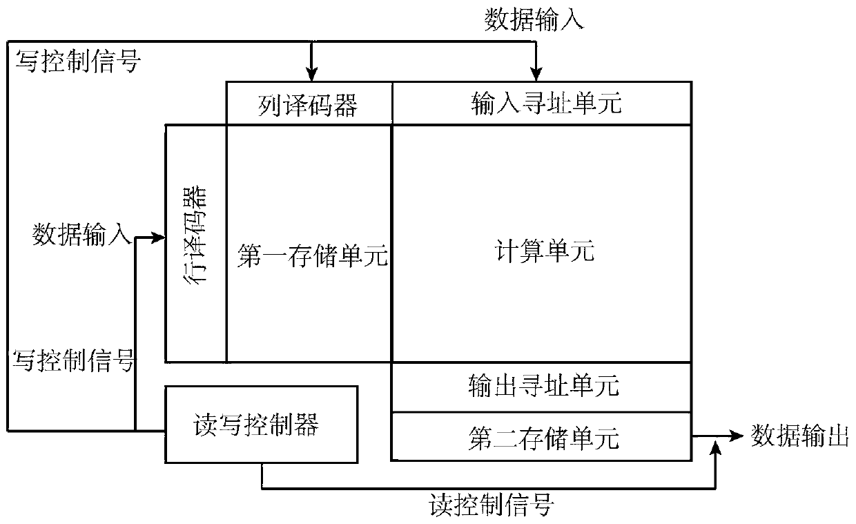
[0073] The spin array module includes more than one spin registers distributed in the array, adjacent spin registers are connected for data transmission, and the spin registers are used for data storage and calculation;

[0074] The peripheral circuit is used to assist the spin register to store and calculate data, including a control module, a selector module, an input register module, an input encoding module, a sense amplifier module, an output register module and a data communication module;

[0075] The control module is used to control the data input and output of the chip and the calculation and storage process;

[0076] The selector module is respectively connected with the spin array module and the control module for s...

Embodiment 2

[0098] An all-in-one chip based on the above spin storage and calculation, such as Figure 8 As shown, a third storage unit may also be included, and the third storage unit is an MRAM storage array, which is used to provide a physically non-copyable function and provide a unique identity for the spin-storage-computing integrated chip.

[0099] It should be further explained that: the third storage unit in this embodiment can exist independently of the first storage unit, or directly use a part of the MRAM storage array in the first storage unit as the third storage unit, which is the same as the first storage unit. A storage unit is connected to the control unit.

[0100]Each chip will inevitably have differences in process parameters during the manufacturing process. The physical non-replicable function is to use the uncontrollable differences introduced by the chip manufacturing process as the characteristic information of the chip. The third storage unit generates a specifi...

Embodiment 3

[0102] A processing terminal including a spin-storage-computing integrated chip includes: a microprocessor and at least one spin-storage-computing integrated chip, and the microprocessor and the spin-storage-computing integrated chip are connected through an interface data line.

[0103] Furthermore, the interface data lines include: serial clock data lines, master device input / slave device output data lines, master device output / slave device input data lines and enable signal data lines;

[0104] The microprocessor transmits the clock signal to the spin-storage-computing integrated chip through the serial clock data line, and the frequency of the clock signal is variable;

[0105] The microprocessor transmits control commands, data to be processed and address signals to the spin memory chip through the master device input / slave device output data line;

[0106] The spin memory chip transmits signals to the microprocessor through the master device output / slave device input dat...


PUM


Abstract

The invention discloses a spin memory and calculation integrated chip, which comprises a spin array module and a peripheral circuit, the spin array module comprises a plurality of spin memories distributed in an array and is used for storing and calculating data; and the spin memory includes a first memory cell composed of a magnetic random access memory (MRAM) array including a magnetic tunnel junction (MTJ) structure for storing data required to be stored for a long time. The peripheral circuit is connected with the spin array module and is used for assisting the spin array module in data storage and calculation. According to the invention, the MRAM is built in the computing core to form the spin memory computing core with storage and computing functions at the same time, the spin memorycomputing chip is formed through the interconnection of the independent spin memory computing cores, and the processing terminal is further formed through the interconnection of the chips. Accordingto the present invention, the problems of a storage wall and a power consumption wall existing in data transmission and processing under a traditional computing framework are effectively solved, and the computing energy efficiency of the system is improved.

Description

technical field [0001] The invention relates to the technical field of spin electronics, and more specifically relates to a spin-storage-computing integrated chip. Background technique [0002] In the traditional von Neumann computing architecture, the memory and the processor are separated, and the two are connected through a data bus, and data processing needs to be transmitted back and forth between the memory and the processor. However, with the rise of big data applications, the transmission and processing of massive data makes the traditional von Neumann computing architecture face the dual challenges of bandwidth and power consumption, which are called storage wall and power consumption wall respectively. In order to solve these two problems, in recent years, inspired by the simultaneous memory and calculation of synapses in the human brain, the Processing-In-Memory (PIM) technology in computer architecture has begun to be widely studied. The traditional integration ...

Claims


Application Information

Patent Timeline
IPC IPC(8): G06F15/78G11C11/16
CPCY02D10/00
Inventor 潘彪康旺赵巍胜
Owner 致真存储(北京)科技有限公司
Why Eureka
Try Eureka