Light-emitting diode epitaxial wafer and manufacturing method thereof

A technology of light-emitting diodes and manufacturing methods, which is applied to electrical components, circuits, semiconductor devices, etc., can solve problems such as poor crystal quality of epitaxial layers, warping of epitaxial layers, and poor wavelength uniformity, so as to improve wavelength uniformity and optimize warping effect

Active Publication Date: 2019-05-21
HC SEMITEK ZHEJIANG CO LTD
View PDF7 Cites 8 Cited by
  • Summary
  • Abstract
  • Description
  • Claims
  • Application Information

AI Technical Summary

Problems solved by technology

[0005] Since the lattice constant of the AlN material (about 0.453) is greater than that of the GaN material (about 0.437), there is still a lattice mismatch between AlN and GaN, and the GaN epitaxial layer grown on the AlN buffer layer will The introduction of a large number of dislocations and tensile stress makes the crystal quality of the grown epitaxial layer poor, and the epitaxial layer will warp, resulting in poor wavelength uniformity of the LED

Method used


Image

  • Light-emitting diode epitaxial wafer and manufacturing method thereof
  • Light-emitting diode epitaxial wafer and manufacturing method thereof
  • Light-emitting diode epitaxial wafer and manufacturing method thereof

Examples


Embodiment Construction

[0030] In order to make the object, technical solution and advantages of the present invention clearer, the implementation manner of the present invention will be further described in detail below in conjunction with the accompanying drawings.

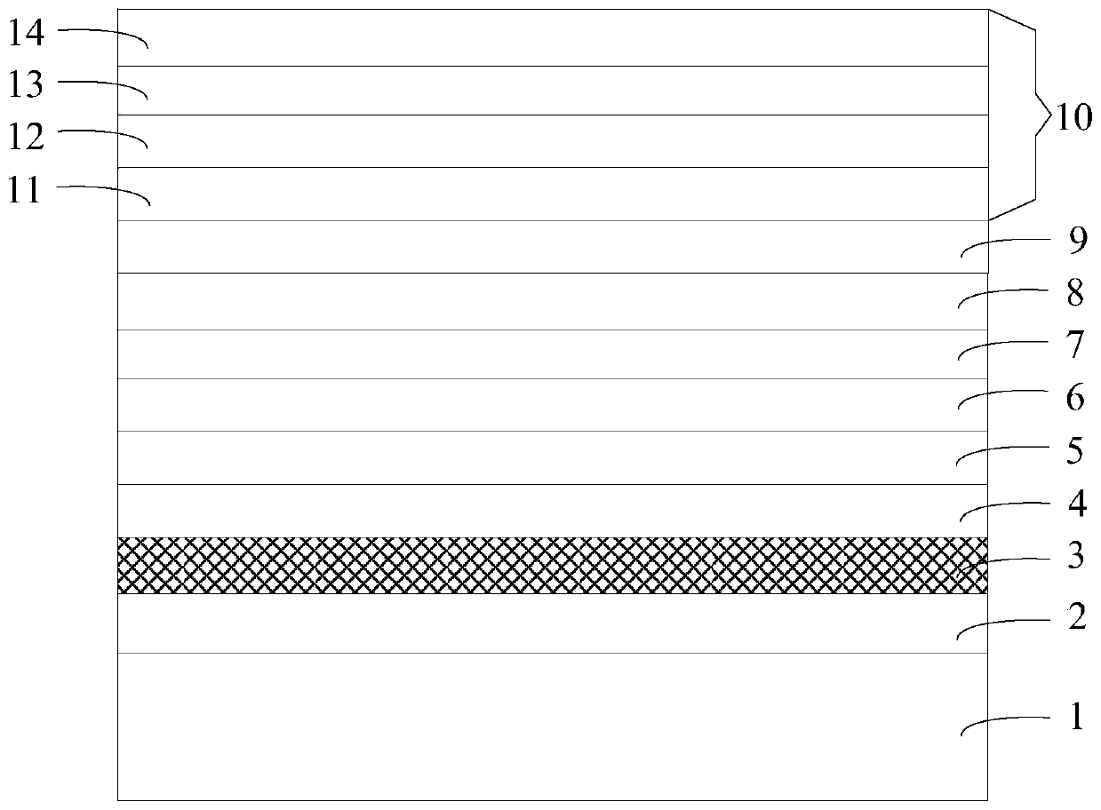
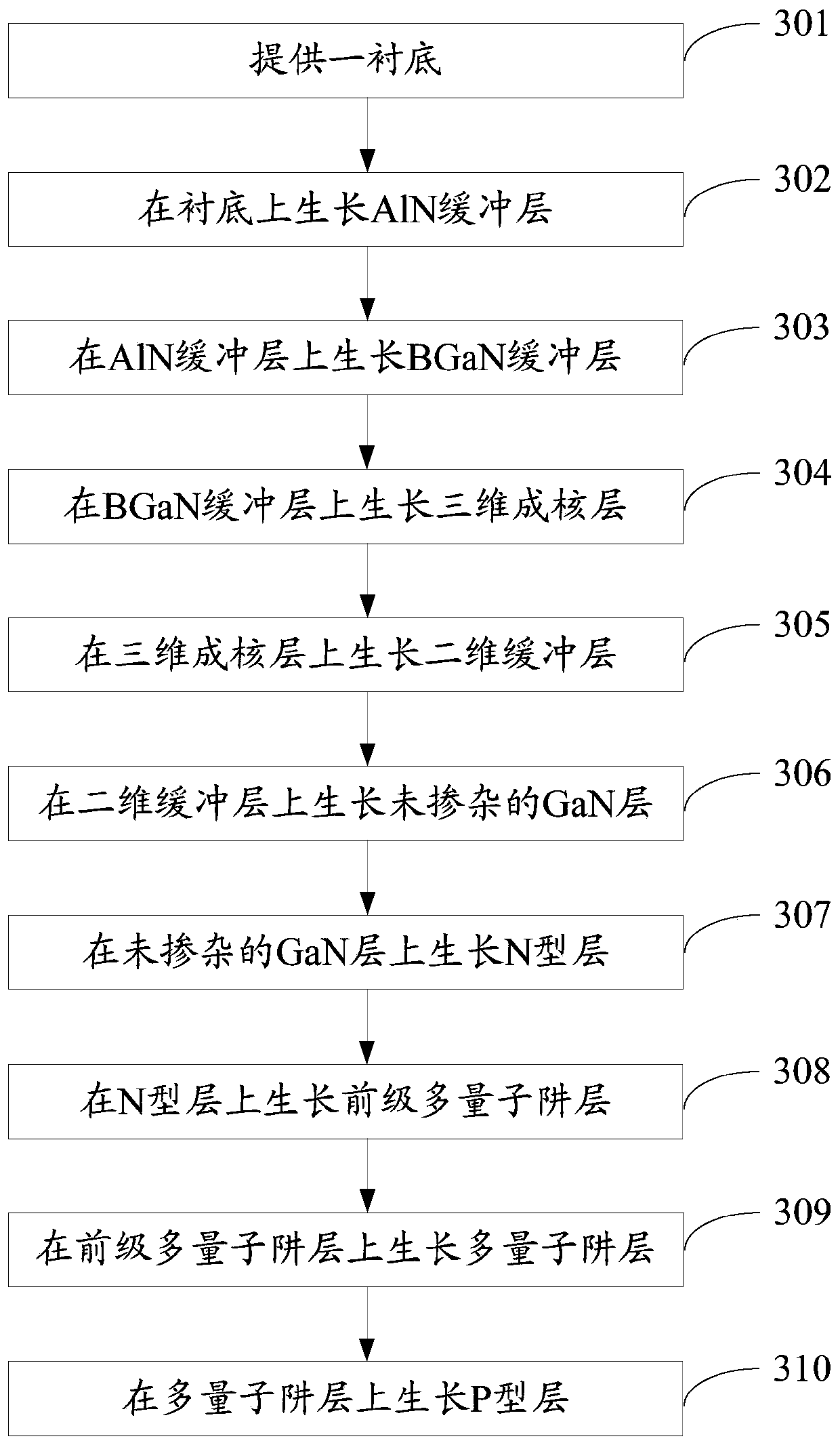
[0031] figure 1 It is a schematic structural diagram of a light-emitting diode epitaxial wafer provided by an embodiment of the present invention, as shown in figure 1 As shown, the light-emitting diode epitaxial wafer includes a substrate 1, and an AlN buffer layer 2, a three-dimensional nucleation layer 4, a two-dimensional recovery layer 5, an undoped GaN layer 6, and an N-type layer 7 grown on the substrate 1 in sequence. , multi-quantum well layer 9 and P-type layer 10.

[0032] The LED epitaxial wafer also includes a BGaN buffer layer 3 disposed between the AlN buffer layer 2 and the three-dimensional nucleation layer 4, and the B component in the BGaN buffer layer 3 gradually decreases along the stacking direction of the LED ep...


PUM


Abstract

The invention discloses a light-emitting diode epitaxial wafer and a manufacturing method thereof, and belongs to the technical field of semiconductors. The light-emitting diode epitaxial wafer comprises a substrate, and an AlN buffer layer, a three-dimensional nucleation layer, a two-dimensional recovery layer, an undoped GaN layer, an N-type layer, a multi-quantum well layer and a P-type layer which are sequentially grown on the substrate, wherein the three-dimensional nucleation layer is a GaN layer; the light-emitting diode epitaxial wafer further comprises a BGaN buffer layer arranged between the AlN buffer layer and the three-dimensional nucleation layer; and the B component in the BGaN buffer layer is gradually reduced in the stacking direction of the light-emitting diode epitaxialwafer. By virtue of the BGaN buffer layer, lattice mismatch between the AlN buffer layer and the GaN epitaxial layer can be gradually reduced, the crystal quality of the grown epitaxial layer is improved, the warping of the epitaxial layer is optimized, and the wavelength uniformity of the LED is improved.

Description

technical field [0001] The invention relates to the technical field of semiconductors, in particular to a light-emitting diode epitaxial wafer and a manufacturing method thereof. Background technique [0002] LED (Light Emitting Diode, Light Emitting Diode) is a semiconductor electronic component that can emit light. As an efficient, environmentally friendly and green new solid-state lighting source, it is being rapidly and widely used, such as traffic lights, car interior and exterior lights, urban landscape lighting, mobile phone backlights, etc. [0003] The epitaxial wafer is the main component of the LED, and the existing GaN-based LED epitaxial wafer includes a sapphire substrate and a GaN epitaxial layer grown on the sapphire substrate. Due to the very serious lattice constant mismatch and thermal mismatch between GaN and sapphire substrate, a large number of dislocations and tensile stress will be introduced into the epitaxial layer. In order to reduce the effects ...

Claims


Application Information

Patent Timeline
Patent Type & Authority Applications(China)
IPC IPC(8): H01L33/12H01L33/00
Inventor 刘旺平乔楠吕蒙普胡加辉李鹏
Owner HC SEMITEK ZHEJIANG CO LTD
Why Eureka
Try Eureka