Wide-spectrum semiconductor active device and manufacturing method thereof

A technology of active devices and semiconductors, applied in semiconductor devices, electrical components, circuits, etc., can solve problems such as concentrated wavelengths, low color rendering index, and narrow half-height width of the spectrum, and achieve the effect of improving injection efficiency

Active Publication Date: 2019-05-14
XI AN JIAOTONG UNIV
View PDF4 Cites 1 Cited by
  • Summary
  • Abstract
  • Description
  • Claims
  • Application Information

AI Technical Summary

Problems solved by technology

[0009] The invention aims to solve the deficiencies in the wide-spectrum application of semiconductor active devices, especially solve the problem of low color rendering index caused by the lack of spectrum in the purple and blue-green light bands of white LEDs, and solve the problem that the spectrum of semiconductor active devices for plant lighting is half. Narrow height and width, wavelength concentration problem, and the need for two kinds of chip integration problems in UV light curing, a wide-spectrum semiconductor active device and its manufacturing method are provided

Method used


Image

  • Wide-spectrum semiconductor active device and manufacturing method thereof
  • Wide-spectrum semiconductor active device and manufacturing method thereof
  • Wide-spectrum semiconductor active device and manufacturing method thereof

Examples


Embodiment 1

[0044] Such as Figure 5 Shown, the manufacture method of the wide-spectrum semiconductor active device provided by the present invention is specifically as follows:

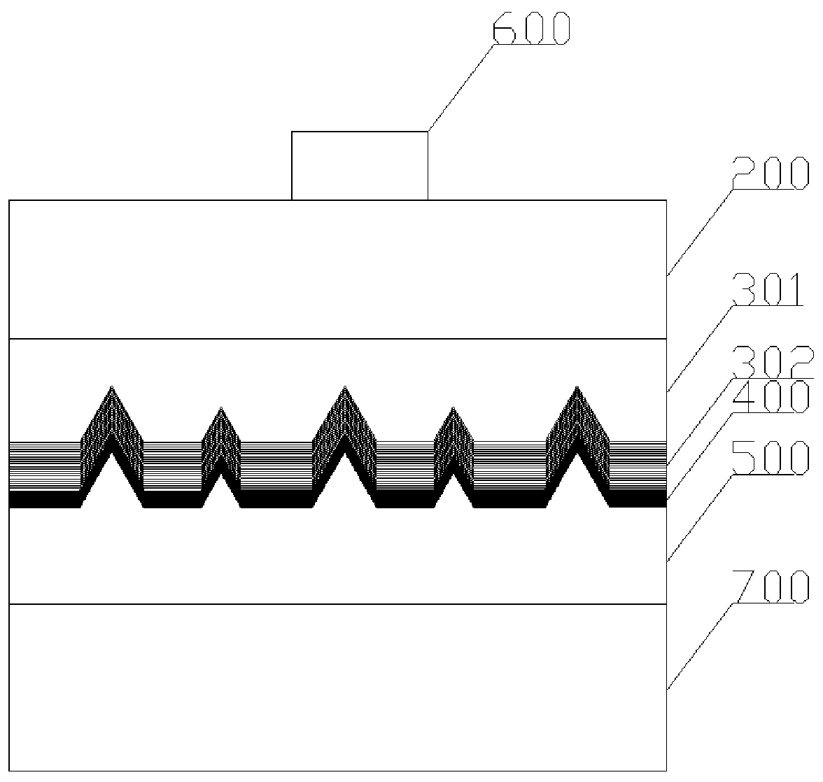
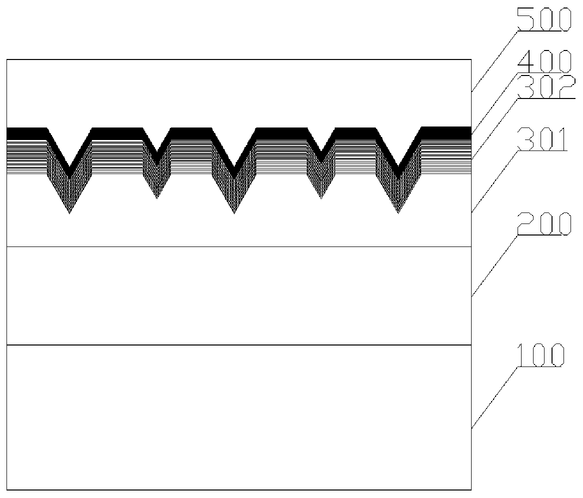
[0045] Step S1, making the epitaxial structure required by the present invention. The epitaxial substrate is one of Si substrate, SiC substrate, ALN substrate, GaN substrate or Sapphire, and the epitaxial structure required by the present invention is epitaxially grown on the substrate by using epitaxial technology such as MOCVD technology or MBE technology. In this embodiment, the GaN material is epitaxially grown by MOCVD on a sapphire substrate. The thickness of the first semiconductor layer 200 is 3um˜6um, the active layer 301 , the electron blocking layer 400 and the second semiconductor layer 500 .

[0046] The active layer includes a two-level modulation structure 301 located 200 between the multi-quantum well structure 302 and the first semiconductor layer, and each level of modulation structure layer ...

Embodiment 2

[0053] Such as Figure 5 Shown, the manufacture method of the wide-spectrum semiconductor active device provided by the present invention is specifically as follows:

[0054] Step S1, making the epitaxial structure required by the present invention. The epitaxial substrate is one of Si substrate, SiC substrate, ALN substrate, GaN substrate or Sapphire, and the epitaxial structure required by the present invention is epitaxially grown on the substrate by using epitaxial technology such as MOCVD technology or MBE technology. In this embodiment, the GaN material is epitaxially grown by MOCVD on a sapphire substrate. The thickness of the first semiconductor layer 200 is 3um˜6um, the active layer 301 , the electron blocking layer 400 and the second semiconductor layer 500 .

[0055] The active layer includes a two-level modulation structure 301 located 200 between the multi-quantum well structure 302 and the first semiconductor layer, and each level of modulation structure layer ...


PUM


Abstract

The invention discloses a wide-spectrum semiconductor active device and a manufacturing method thereof; the active device comprises an epitaxial substrate and a multi-layer semiconductor structure formed on the epitaxial substrate; the multi-layer semiconductor structure comprises a first semiconductor layer, an active layer and a second semiconductor layer which are sequentially formed on the epitaxial substrate, and a first electrode and a second electrode which are electrically connected with the first semiconductor layer and the second semiconductor layer in a direct or indirect mode respectively. The manufacturing method comprises the following steps of manufacturing the epitaxial structure; exposing all or part of the first semiconductor layer, manufacturing the first electrode on the exposed first semiconductor layer, and manufacturing the second electrode on the surface of the second semiconductor layer. According to the method, the wide spectrum and multi-spectral radiation ofthe semiconductor active device can be realized.

Description

technical field [0001] The invention belongs to the technical field of semiconductors, in particular to a wide-spectrum semiconductor active device and a manufacturing method thereof. Background technique [0002] Semiconductor active devices have developed rapidly in recent years, among which the semiconductor light radiation device of the III-V compound semiconductor material system is the most prominent, and the typical representative materials are AlN, GaN, InN and their combinations of ternary or quaternary compounds , the theoretical band gap ranges from 6.2eV to 0.7eV, and the optical radiation wavelength can cover deep ultraviolet to infrared bands. At present, the InGaN / GaN series of blue-green LEDs have set off a revolution in lighting technology. Ultraviolet and ultraviolet LEDs based on AlGaN materials play a huge role in the fields of ultraviolet curing, ultraviolet sterilization and medicine. Blue-green light and ultraviolet LD have also shown great applicati...

Claims


Application Information

Patent Timeline
Patent Type & Authority Applications(China)
IPC IPC(8): H01L33/06H01L33/02H01L33/32H01L33/00
Inventor 云峰苏喜林李虞锋张敏妍郭茂峰李琨赵丁
Owner XI AN JIAOTONG UNIV
Why Eureka
Try Eureka