Check patentability & draft patents in minutes with Patsnap Eureka AI!

GaN-based lithium-emitting diode epitaxial wafer and fabrication method thereof

A technology of light-emitting diodes and epitaxial wafers, applied in electrical components, circuits, semiconductor devices, etc., can solve the problems of reduced electron and hole radiation recombination efficiency, low energy level, weak electron blocking effect, etc., to reduce electron overflow, Improve luminous efficiency and increase the effect of blocking effect

Active Publication Date: 2019-05-21
HC SEMITEK ZHEJIANG CO LTD
View PDF4 Cites 4 Cited by
  • Summary
  • Abstract
  • Description
  • Claims
  • Application Information

AI Technical Summary

Problems solved by technology

[0003] In the process of realizing the present invention, the inventors found that the prior art has at least the following problems: the energy level of the AlGaN electron blocking layer is low, the blocking effect on electrons is weak, and a large number of electrons in the MQW layer overflow to the P-type doping GaN layer, resulting in greatly reduced radiative recombination efficiency of electrons and holes

Method used


Image

  • GaN-based lithium-emitting diode epitaxial wafer and fabrication method thereof
  • GaN-based lithium-emitting diode epitaxial wafer and fabrication method thereof
  • GaN-based lithium-emitting diode epitaxial wafer and fabrication method thereof

Examples


Embodiment Construction

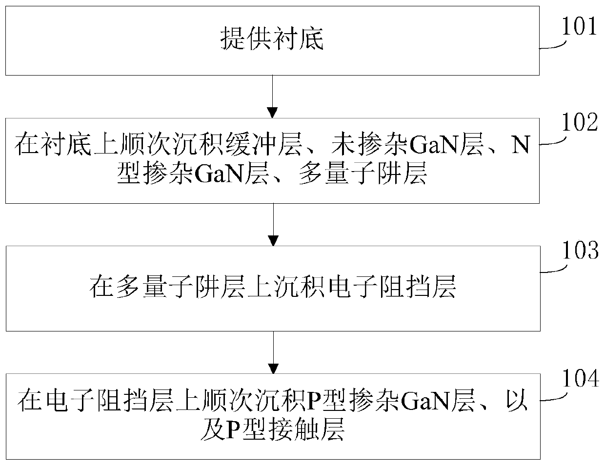
[0026] In order to make the object, technical solution and advantages of the present invention clearer, the implementation manner of the present invention will be further described in detail below in conjunction with the accompanying drawings.

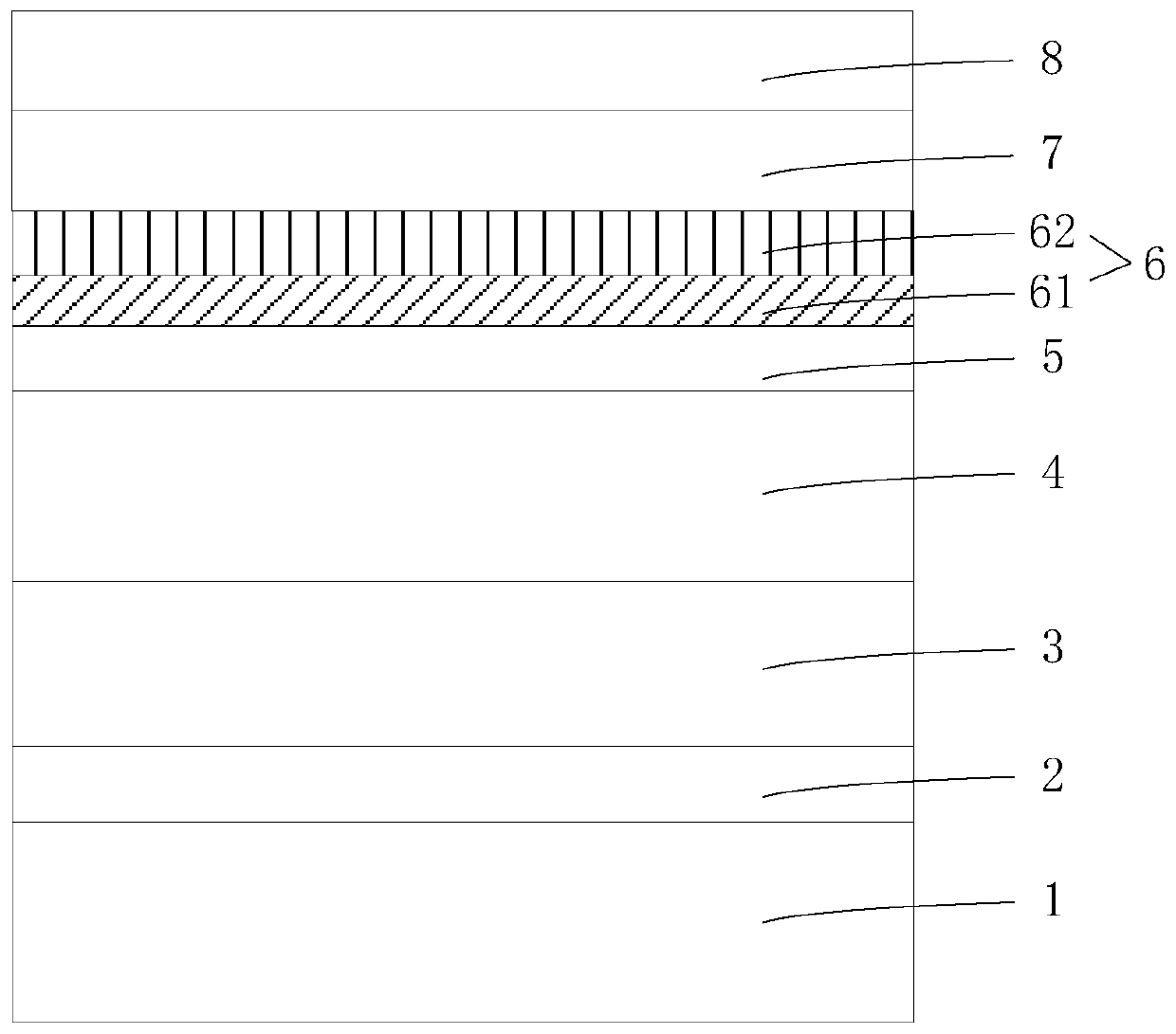
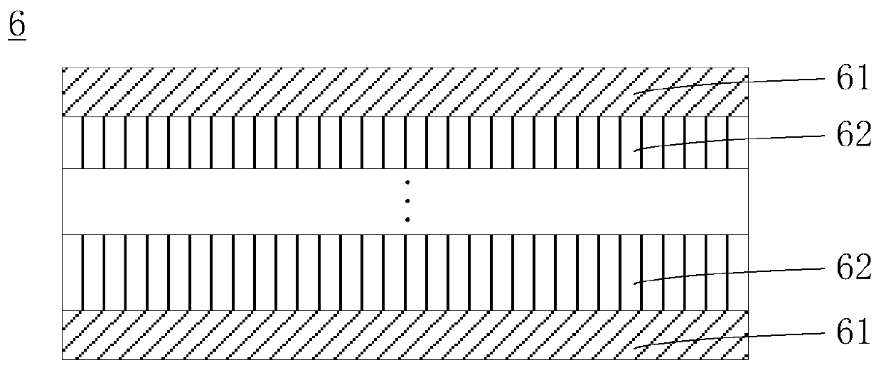
[0027] figure 1 A GaN-based light-emitting diode epitaxial wafer provided by an embodiment of the present invention is shown. see figure 1 , the light-emitting diode epitaxial wafer includes: a substrate 1, and a buffer layer 2 deposited sequentially on the substrate 1, an undoped GaN layer 3, an N-type doped GaN layer 4, a multi-quantum well layer 5, and an electron blocking layer 6. P-type doped GaN layer 7 and P-type contact layer 8 . Wherein, the electron blocking layer 6 includes at least one AlN sublayer 61 and at least one MgN sublayer 62 laminated.

[0028] Through the electron blocking layer 6 comprising at least one AlN sublayer 61 and at least one MgN sublayer 62 stacked, compared to the conventional AlGaN electron blocki...


PUM

PropertyMeasurementUnit
Thicknessaaaaaaaaaa

Abstract

The invention discloses a GaN-based lithium-emitting diode epitaxial wafer and a fabrication method thereof, and belongs to the field of a GaN-based lithium-emitting diode. The light-emitting diode epitaxial wafer comprises a substrate and a buffer layer, a non-doped GaN layer, an N-type doping GaN layer, a multi-quantum well layer, an electron blocking layer, a P-type doped GaN layer and a P-typecontact layer which are sequentially deposited on the substrate, and the electron blocking layer comprises at least one AIN sub-layer and at least one MgN sub-layer which are laminated.

Description

technical field [0001] The invention relates to the field of GaN-based light-emitting diodes, in particular to a GaN-based light-emitting diode epitaxial wafer and a preparation method thereof. Background technique [0002] A GaN (gallium nitride)-based LED (Light Emitting Diode, light emitting diode), also called a GaN-based LED chip, generally includes an epitaxial wafer and electrodes prepared on the epitaxial wafer. The epitaxial wafer usually includes: a substrate, a buffer layer sequentially stacked on the substrate, an undoped GaN layer, an N-type GaN layer, an MQW (Multiple Quantum Well, multiple quantum well) layer, an electron blocking layer, a P-type doped Doped GaN layer and contact layer. When a current is injected into the GaN-based LED, the electrons in the N-type region such as the N-type GaN layer and the holes in the P-type region such as the P-type doped GaN layer enter the MQW active region and recombine to emit visible light. Wherein, the material of t...

Claims


Application Information

Patent Timeline
IPC IPC(8): H01L33/14H01L33/06H01L33/32H01L33/00
Inventor 王曼周飚胡加辉
Owner HC SEMITEK ZHEJIANG CO LTD
Features
  • R&D
  • Intellectual Property
  • Life Sciences
  • Materials
  • Tech Scout
  • Unparalleled Data Quality
  • Higher Quality Content
  • 60% Fewer Hallucinations
Learn More