Preparation method and application of total inorganic perovskite film
An inorganic calcium and thin-film technology, which is applied in semiconductor/solid-state device manufacturing, electrical components, electric solid-state devices, etc., can solve the problem of insufficient performance of light-emitting diodes, multi-surface defects of all-inorganic perovskite thin films, and limit the improvement of device performance and other issues, to save material and time costs, facilitate carrier recombination, improve brightness and efficiency
- Summary
- Abstract
- Description
- Claims
- Application Information
AI Technical Summary
Problems solved by technology
Method used
Image
Examples
Embodiment 1
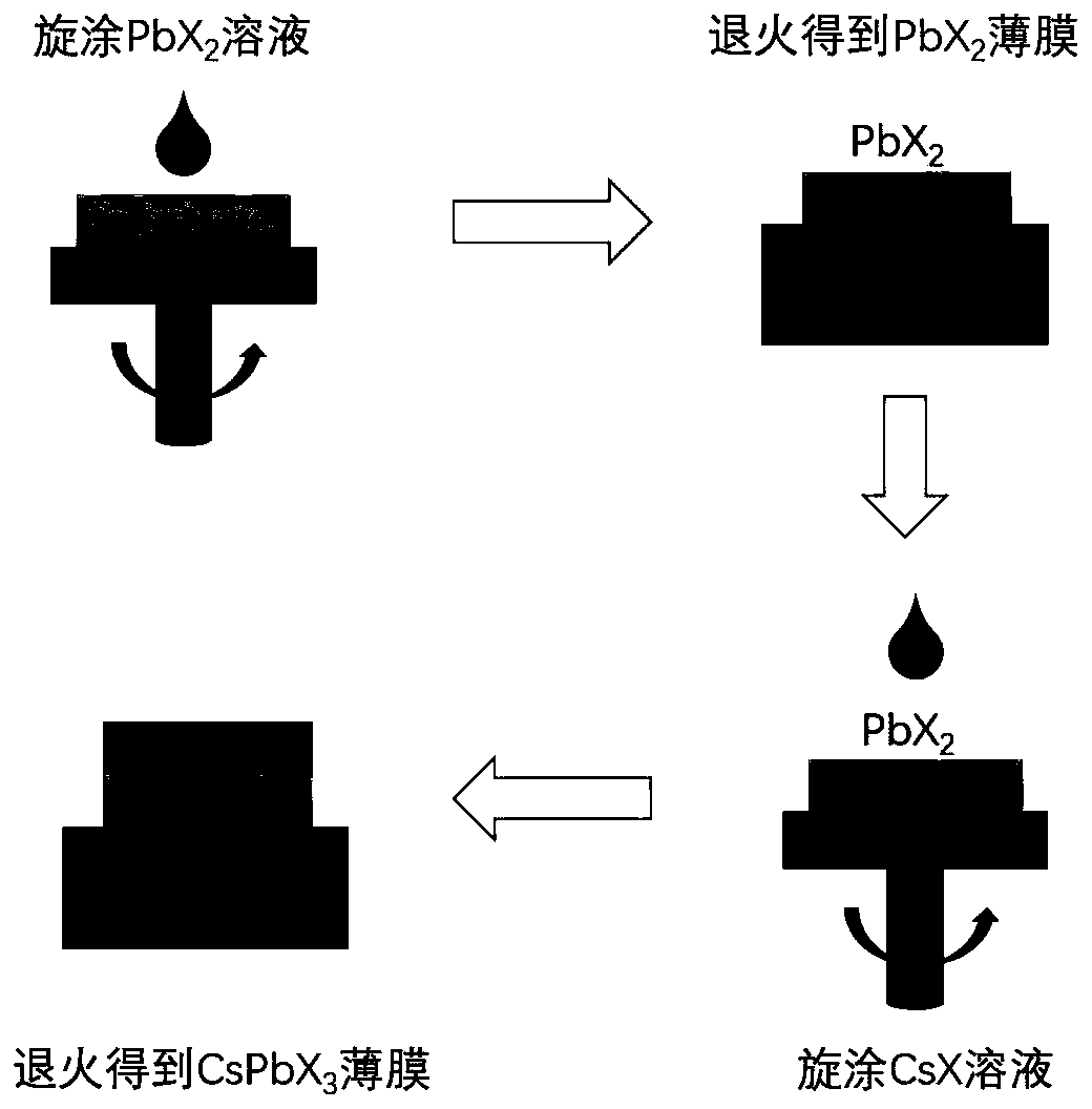
[0027] Reference now figure 1 , Given a kind of CsPbBr under nitrogen atmosphere 3 The preparation method of all-inorganic perovskite film specifically includes the following steps:
[0028] (1) Configure PbBr 2 Solution, PbBr 2 Dissolve in DMSO, the concentration is 100mg / ml, stir well to dissolve;
[0029] (2) Prepare the CsBr solution, dissolve CsBr in methanol with concentrations of 5, 10, and 15 mg / ml, and stir well until it dissolves;
[0030] (3) The solution obtained in step (1) was spin-coated on the substrate at 3000 rpm for 45 seconds, and then annealed at 80 degrees for 5 minutes to obtain PbBr 2 film;
[0031] (4) The three different concentration solutions obtained in step (3) were spin-coated on the PbBr obtained in step (2) at 2500 rpm. 2 On the film, the time is 45s, and then annealed at 80 degrees for 2 minutes to obtain CsPbBr 3 All inorganic perovskite film.
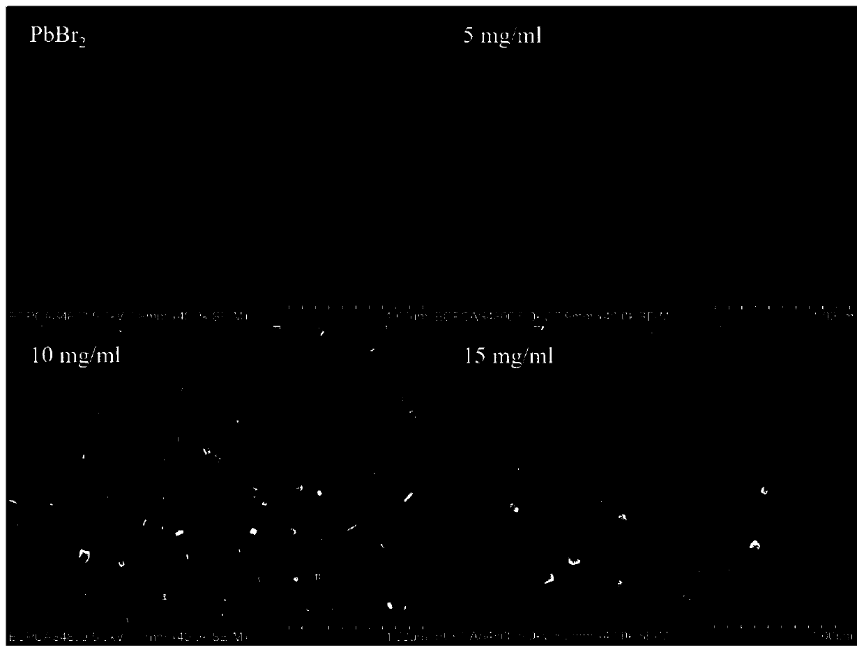
[0032] figure 2 Shown is the prepared PbBr 2 CsPbBr obtained by spin coating film and different concentrati...
Embodiment 2
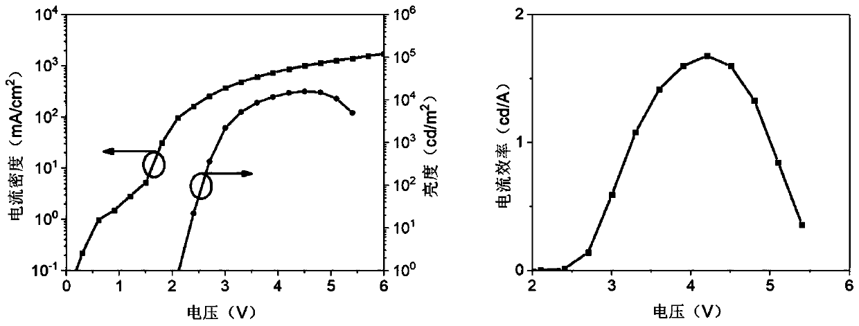
[0034] We use the perovskite film obtained in Example 1 as the active light-emitting layer for the preparation of all-inorganic light-emitting diodes. The structure of the light-emitting diode device is ITO / PEDOT:PSS / CsPbBr 3 / Bphen / LiF / Ag, specifically including the following steps:
[0035] (1) Use special glass cleaner, deionized water, and alcohol to ultrasonically clean the ITO glass substrate in sequence, dry it with nitrogen after cleaning, and then treat the substrate with an ultraviolet ozone processor for 15 minutes;
[0036] (2) PEDOT:PSS was spin-coated on the glass substrate obtained in step (1) as a hole transport layer at 3500 rpm for 30 seconds, and then annealed at 150 degrees for 10 minutes;
[0037] (3) The substrate obtained in step (2) is transferred into a glove box in a nitrogen atmosphere to prepare the perovskite luminescent layer. The preparation method is the same as that in Example 1. The CsPbBr 3 The film is deposited on the hole transport layer PEDOT:PSS,...
PUM
 Abstract
Description
Claims
Application Information


