
Method for passivating single-crystal surface by tungsten oxide

A tungsten oxide, single crystal silicon technology, applied in sustainable manufacturing/processing, electrical components, climate sustainability, etc., can solve problems such as inability to apply solar cell technology, instability, etc., to achieve high film purity and density, The effect of unique film structure and performance and simple film formation method

Inactive Publication Date: 2019-05-17
ZHEJIANG NORMAL UNIVERSITY
View PDF5 Cites 0 Cited by
  • Summary
  • Abstract
  • Description
  • Claims
  • Application Information

AI Technical Summary

Problems solved by technology

However, since this passivation method is extremely unstable
Therefore, it cannot be used in solar cell technology, but only in some tests

Method used


Image

  • Method for passivating single-crystal surface by tungsten oxide
  • Method for passivating single-crystal surface by tungsten oxide
  • Method for passivating single-crystal surface by tungsten oxide

Examples


Embodiment Construction

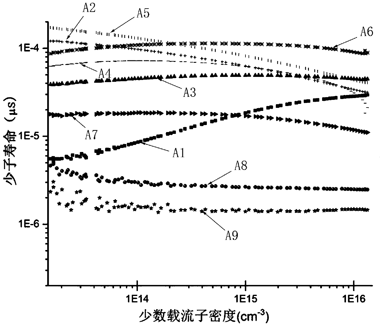
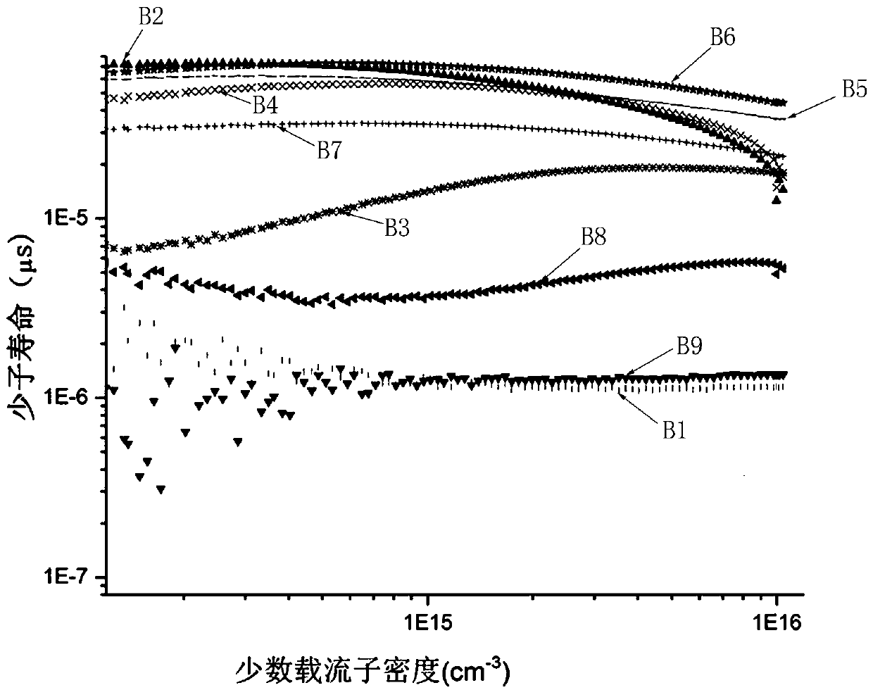
[0013] The samples used in the present invention are N type single crystal non-polished silicon chips with an area of ​​40 mm*40 mm and a thickness of 190 μm, and the resistivity is 1-5 Ω·cm. The specific connotation of the present invention will be further elaborated below in conjunction with specific embodiments.

[0014] (1) No silicon dioxide layer:

[0015] 1. Select 9 pieces of N type single crystal silicon wafers as samples.

[0016] 2. The silicon wafer is uniformly cleaned by removing the damaged layer and RCA method, and ultrasonically cleaning with deionized water (DIW) for 2 minutes between each step. The specific steps are as follows:

[0017] 1) Ultrasonic cleaning with acetone for 10 minutes;

[0018] 2) Ultrasonic cleaning with absolute ethanol for 10 minutes;

[0019] 3) Prepare a KOH solution with a concentration of 25%, and heat it in a water bath at 80°C for 20 minutes;

[0020] 4) with (29%) NH 4 OH:(30%)H 2 o 2 :DIW=1:1:5 Prepare cleaning solution,...


PUM


Abstract

The invention discloses a method for passivating a single-crystal surface by tungsten oxide. The method comprises the steps of washing a silicon wafer to obtain a clean and hydrophobic silicon wafer surface, placing the silicon wafer in concentrated nitric acid to grow a layer of silicon dioxide which does not exceed 1 nanometer so as to isolate contact between the silicon wafer surface and outside; placing a layer of tungsten oxide thin film on the silicon wafer surface; and annealing in a tubular furnace at 200-250 DEG C with nitrogen. According to the method, tungsten oxide powder is deposited on the silicon wafer surface by an evaporation method, and the method has the advantages of simple film formation method, high purity and compactness of the thin film, film structure, unique performance and the like.

Description

technical field [0001] The invention belongs to the technical field of manufacturing solar-grade silicon wafers, and particularly relates to the surface passivation problem of single crystal silicon. By adding tungsten oxide (WO 3 ) to achieve effective passivation of silicon wafers, thereby improving the lifetime of minority carriers. Background technique [0002] On the surface of the silicon wafer, the periodicity of the crystal is destroyed to generate dangling bonds, so that there are a large number of defect levels in the band gap on the crystal surface; in addition, dislocations, chemical residues, and deposition of surface metals will all introduce defect levels. These make the surface of the silicon wafer a recombination center. The surface recombination rate has a great influence on the performance of solar cells. Studies have shown that when the recombination rate of the back is increased from 10cm / s to 10 3 cm / s and 10 5 At cm / s, the efficiency of solar cells...

Claims


Application Information

Patent Timeline
IPC IPC(8): H01L31/18H01L31/0216
CPCY02P70/50
Inventor 黄仕华芮哲陆肖励
Owner ZHEJIANG NORMAL UNIVERSITY
Learn More