Method for preparing polycrystalline silicon passivation contact structure through tubular PECVD

A contact structure and polysilicon technology, which is applied in the field of solar cells, can solve the problems of increasing production costs, reducing battery yield, and long process time, so as to save costs, improve yield, and reduce the number of processes.

Active Publication Date: 2019-05-24
NINGBO INST OF MATERIALS TECH & ENG CHINESE ACADEMY OF SCI
View PDF8 Cites 19 Cited by
  • Summary
  • Abstract
  • Description
  • Claims
  • Application Information

AI Technical Summary

Problems solved by technology

At the same time, the price of related equipment is relatively high, which increases the production cost
[0022] 3) Long process time: the total time for preparing silicon oxide, intrinsic polysilicon, phosphorus diffusion and other steps is more than 280 minutes, which is very long and greatly reduces the battery yield

Method used


Image

  • Method for preparing polycrystalline silicon passivation contact structure through tubular PECVD
  • Method for preparing polycrystalline silicon passivation contact structure through tubular PECVD

Examples


Embodiment 1

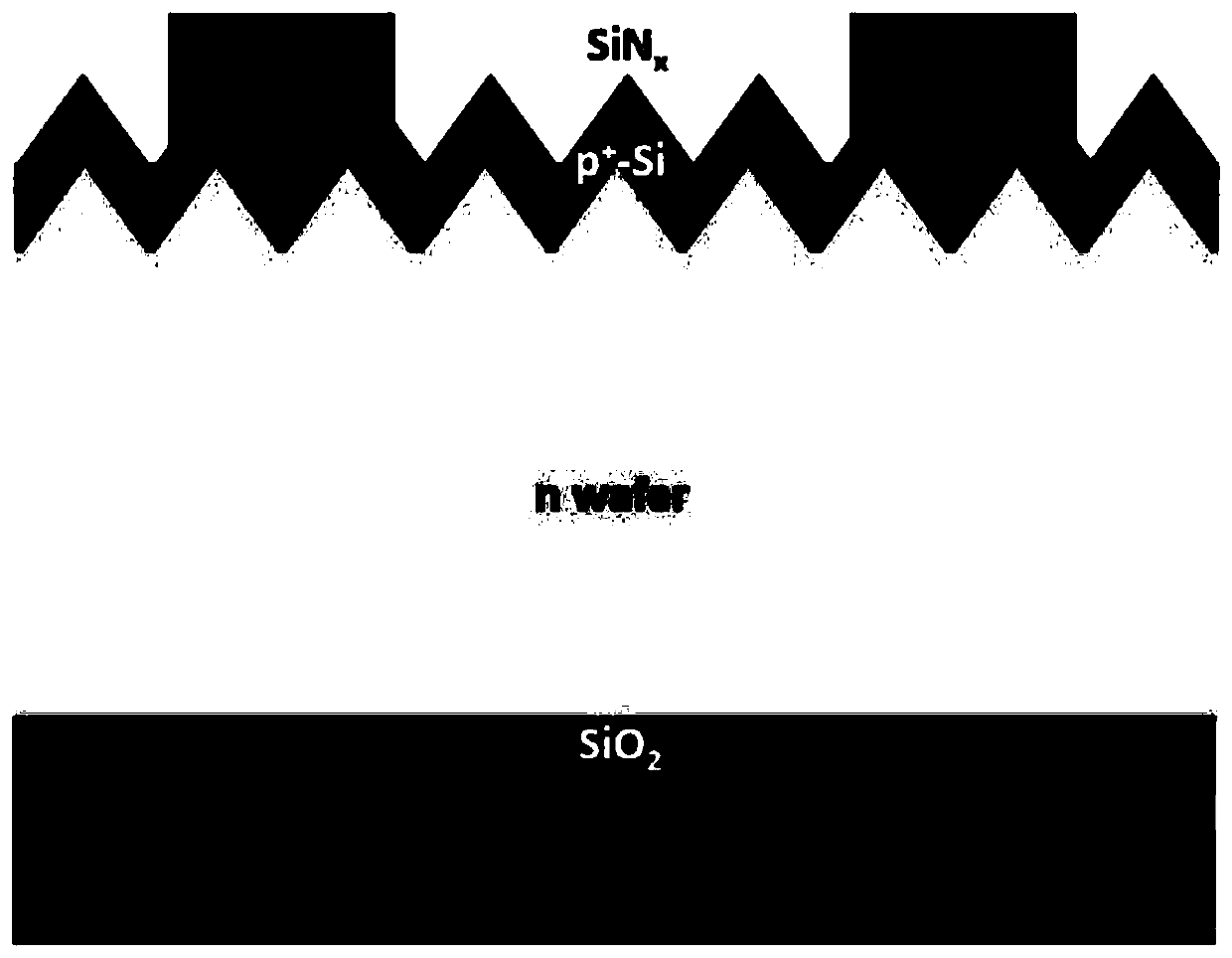
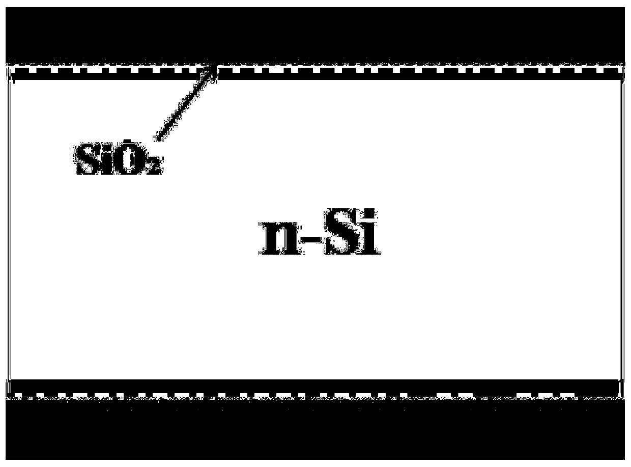
[0056] Using the n-type silicon wafer, the surface damage layer is removed, and the same structure is plated on both sides. The specific processing is as follows:

[0057] 1. Put the silicon wafer into the graphite boat after cleaning;

[0058] 2. Deposition of silicon oxide: substrate temperature 400 o C, with laughing gas (N 2 O) is the reaction gas, the flow rate is 3000sccm, the air pressure is 200Pa, the deposition power is 2000W, the radio frequency on-off ratio is 2ms: 10ms, and the deposition time is 120 seconds;

[0059] 3. Deposit I layer of phosphorus-doped amorphous silicon film on the silicon oxide layer: substrate temperature 600 o C, SiH 4 :H 2 : PH 3 =1500sccm: 10000sccm: 1500sccm, the air pressure is 250Pa, the deposition power is 2000W, the RF on-off ratio is 3ms: 45ms, and the deposition time is 600 seconds;

[0060] 4. Deposit II layer of phosphorus-doped amorphous silicon film on layer I of phosphorus-doped amorphous silicon film: substrate temperat...

Embodiment 2

[0064] Using the n-type silicon wafer, the surface damage layer is removed, and the same structure is plated on both sides. The specific processing is as follows:

[0065] 1. Put the silicon wafer into the graphite boat after cleaning;

[0066] 2. Deposition of silicon oxide: substrate temperature 400 o C, as carbon dioxide (CO 2 ) is the reactive gas, the flow rate is 5000sccm, the air pressure is 220Pa, the deposition power is 2500W, the radio frequency on-off ratio is 2ms:30ms, and the deposition time is 120 seconds;

[0067] 3. Deposition I layer of phosphorus-doped amorphous silicon film: substrate temperature 500 o C, SiH 4 :H 2 : PH 3 =1000sccm: 10000sccm: 1000sccm, the air pressure is 250Pa, the deposition power is 2000W, the RF on-off ratio is 3ms: 75ms, and the deposition time is 500 seconds;

[0068] 4. Deposition II layer of phosphorus-doped amorphous silicon film: substrate temperature 500 o C, SiH 4 :H 2 : PH 3 =1000sccm: 10000sccm: 1000sccm, the air p...

Embodiment 3

[0072] Using the n-type silicon wafer, the surface damage layer is removed, and the same structure is plated on both sides. The specific processing is as follows:

[0073] 1. Put the silicon wafer into the graphite boat after cleaning;

[0074] 2. Deposition of silicon oxide: substrate temperature 400 o C, with laughing gas (N 2 O) is the reaction gas, the flow rate is 3000sccm, the air pressure is 200Pa, the deposition power is 2000W, the radio frequency on-off ratio is 2ms: 10ms, and the deposition time is 120 seconds;

[0075] 3. Deposition I layer of boron-doped amorphous silicon film: substrate temperature 600 o C, SiH 4 :H 2 :B 2 H 6 =1500sccm: 2000sccm: 1500sccm, the air pressure is 250Pa, the deposition power is 1800W, the RF on-off ratio is 3ms: 45ms, and the deposition time is 600 seconds;

[0076] 4. Deposition II layer of boron-doped amorphous silicon film: substrate temperature 600 o C, SiH 4 :H 2 :B 2 H 6 =1600sccm: 10000sccm: 1600sccm, the air press...


PUM

PropertyMeasurementUnit
thicknessaaaaaaaaaa
thicknessaaaaaaaaaa
thicknessaaaaaaaaaa

Abstract

The invention discloses a method for preparing a polycrystalline silicon passivation contact structure through tubular PECVD. The method includes the following steps that: a doped amorphous silicon film is prepared on the surface of an oxide and / or nitride of silicon through adopting the tubular PECVD; and a polycrystalline silicon passivation contact structure is obtained through high-temperaturecrystallization annealing. With the method of the invention adopted, a high-quality TOPCon structure can be prepared; the passivation efficiency of the TOPCon structure is completely equivalent to that of an LPCVD technology, in particular, the iVoc of an n-type silicon wafer adopting n-type TOPCon double-sided passivation can reach 720 to 750mV; and a production process can be greatly simplified.

Description

technical field [0001] The invention relates to the technical field of solar cells, in particular to a method for preparing a polysilicon passivation contact (TOPCon) structure by tubular PECVD. Background technique [0002] The tunneling oxygen / polysilicon passivation contact (TOPCon) solar cell is a new type of silicon solar cell proposed by the Fraunhofer Institute in Germany since 2013. The back of the cell is covered with an ultra-thin silicon oxide layer with a thickness of less than 2nm, and then covered with a layer of doped amorphous silicon, and then annealed at high temperature to form heavily doped polysilicon. Taking n-type phosphorus doped TOPCon as an example, the basic structure of the battery is as follows figure 1 As shown, the typical passivation plate structure is as follows figure 2 shown. The backside structure of the battery is sequentially n-type silicon wafer / ultra-thin tunnel oxide layer / n+ polysilicon layer / metal electrode layer. Depending on ...

Claims


Application Information

Patent Timeline
Patent Type & Authority Applications(China)
IPC IPC(8): H01L31/18H01L31/068
CPCY02E10/546Y02P70/50
Inventor 曾俞衡闫宝杰叶继春廖明墩
Owner NINGBO INST OF MATERIALS TECH & ENG CHINESE ACADEMY OF SCI
Why Eureka
Try Eureka